Official Paper

GATE EC 2022 Official Paper (Previous Year Paper)

65 questions · 180 minutes · with answers · free

General Aptitude (10 questions)

1

Mr. X speaks _________ Japanese _________ Chinese.

  1. ((a))

    neither / or

  2. ((b))

    either / nor

  3. ((c))

    neither / nor

  4. ((d))

    also / but

Show Answer
Answer: ((c))

neither / nor

The correct answer is 'neither / nor'.

Key Points

  • In the given blanks, it can be understood that conjunctions are to be filled.
  • We will use the alternative conjunctions 'neither/nor' as we can understand that Mr. X is unable to speak both languages.

The complete sentence will be: Mr. X speaks neither Japanese nor Chinese.

  • Hence, option 3 is the correct answer.

Additional Information

  • When we have to choose one out of two given alternatives, we use alternative conjunctions such as either/or, neither/nor, else, or otherwise.
  • For eg.- Walk slowly on the ice, otherwise, you'll fall.
2

A sum of money is to be distributed among P, Q, R, and S in the proportion 5 ∶ 2 ∶ 4 ∶ 3, respectively.

If R gets Rs. 1000 more than S, what is the share of Q (in Rs.)?

  1. ((a))

    500

  2. ((b))

    1000

  3. ((c))

    1500

  4. ((d))

    2000

Show Answer
Answer: ((d))

2000

Given:

The ratio of distributed money among P, Q, R, and S in the proportion 5 ∶ 2 ∶ 4 ∶ 3, respectively.

R gets Rs. 1000 more than S.

Calculation:

The ratio of distributed money,

P : Q : R : S = 5 ∶ 2 ∶ 4 ∶ 3

Suppose, P gets Rs. 5x, Q gets Rs. 2x, R gets Rs. 4x, and S gets Rs. 3x.

According to the question, R gets Rs. 1000 more than S.

Therefore, 4x - 3x = 1000

⇒ x = 1000

∴ Q gets = 2 × 1000 = Rs. 2000

∴ The share of Q (in Rs.) is Rs. 2000

3

A trapezium has vertices marked as P, Q, R and S (in that order anticlockwise). The side PQ is parallel to side SR.

Further, it is given that, PQ = 11 cm, QR = 4 cm, RS = 6 cm and SP = 3 cm.

What is the shortest distance between PQ and SR (in cm)?

  1. ((a))

    1.80

  2. ((b))

    2.40

  3. ((c))

    4.20

  4. ((d))

    5.76

Show Answer
Answer: ((b))

2.40

Given:

A trapezium has vertices marked as P, Q, R, and S (in that order anticlockwise), and PQ || RS

PQ = 11 cm, QR = 4 cm, RS = 6 cm and SP = 3 cm

Formula used:

For a right-angle triangle, Perpendicular=(Hypotenuse2Base2)Perpendicular = \sqrt{(Hypotenuse^2 - Base^2)}

Calculation:

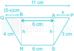
Let's draw the diagram according to the question,

Here, the trapezium has vertices marked as P, Q, R, and S (in that order anticlockwise), and PQ || RS

PQ = 11 cm, QR = 4 cm, RS = 6 cm and SP = 3 cm

Draw two perpendiculars from point R and point S that connect to PQ at point B and point A respectively are shown in the above diagram.

Therefore, △BCQ and △ASP are both right-angle triangles. [∠QBR = ∠PAS = 90º]

Here, BR = AS = h [PQ || RS]

PQ = 11 cm and RS = 6 cm

Suppose, PA = x

∴ QB = 11 - (6 + x) = (5 - x)

Therefore, h=QR2QB2=SP2PA2h = \sqrt{QR^2 - QB^2} = \sqrt{SP^2 - PA^2}

⇒ h=42(5x)2=32x2h = \sqrt{4^2 - (5 - x)^2} = \sqrt{3^2 - x^2}

⇒ 42(5x)2=32x2\sqrt{4^2 - (5 - x)^2} = \sqrt{3^2 - x^2}

⇒ 16 - (5 - x)2 = 9 - x2

⇒ 16 - (25 - 10x + x2) = 9 - x2

⇒ 16 - 25 + 10x - x2 = 9 - x2

⇒ 10x = 9 - 10 + 25 = 18

⇒ x = 18/10 = 1.8

Now, h=321.82h = \sqrt{3^2 - 1.8^2}

⇒ h=93.24=5.76h = \sqrt{9 - 3.24} = \sqrt{5.76} = 2.4 cm

∴ The shortest distance between PQ and SR (in cm) is 2.4 cm.

4

The figure shows a grid formed by a collection of unit squares. The unshaded unit square in the grid represents a hole.

What is the maximum number of squares without a “hole in the interior” that can be formed within the 4 × 4 grid using the unit squares as building blocks?

  1. ((a))

    15

  2. ((b))

    20

  3. ((c))

    21

  4. ((d))

    26

Show Answer
Answer: ((b))

20

According to the question, 

Total number of squares = 16

Number of squares without hole,

4 × 4 - 1 = 16 - 1 = 15,

∴ the total number of 1 × 1 squares (without hole) = 15

Now,

the total number of 2 × 2 squares (without hole) = 5

Total number of squares = 15 + 5 = 20

5

An art gallery engages a security guard to ensure that the items displayed are protected. The diagram below represents the plan of the gallery where the boundary walls are opaque. The location the security guard posted is identified such that all the inner space (shaded region in the plan) of the gallery is within the line of sight of the security guard.

If the security guard does not move around the posted location and has a 360° view, which one of the following correctly represents the set of ALL possible locations among the locations P, Q, R and S, where the security guard can be posted to watch over the entire inner space of the gallery.

  1. ((a))

    P and Q

  2. ((b))

    Q

  3. ((c))

    Q and S

  4. ((d))

    R and S

Show Answer
Answer: ((c))

Q and S

If a person will stand on ‘P’ then he/she can’t see the visibility side of R and vice versa.

But if the security guard will be stand at Q and S then he will be whole 360°

Security guard posting at Q and S can watch entire space of gallery.

6

Mosquitoes pose a threat to human health. Controlling mosquitoes using chemicals may have undesired consequences. In Florida, authorities have used genetically modified mosquitoes to control the overall mosquito population. It remains to be seen if this novel approach has unforeseen consequences.

Which one of the following is the correct logical inference based on the information in the above passage?

  1. ((a))

    Using chemicals to kill mosquitoes is better than using genetically modified mosquitoes because genetic engineering is dangerous

  2. ((b))

    Using genetically modified mosquitoes is better than using chemicals to kill mosquitoes because they do not have any side effects

  3. ((c))

    Both using genetically modified mosquitoes and chemicals have undesired consequences and can be dangerous

  4. ((d))

    Using chemicals to kill mosquitoes may have undesired consequences but it is not clear if using genetically modified mosquitoes has any negative consequence

Show Answer
Answer: ((d))

Using chemicals to kill mosquitoes may have undesired consequences but it is not clear if using genetically modified mosquitoes has any negative consequence

The correct answer is 'Using chemicals to kill mosquitoes may have undesired consequences but it is not clear if using genetically modified mosquitoes has any negative consequence'.

Key Points

  • Let's refer to the passage:
  • 'In Florida, authorities have used genetically modified mosquitoes to control the overall mosquito population.'
  • 'It remains to be seen if this novel approach has unforeseen consequences.'
  • From the above-mentioned statements, it is evident that the correct logical inference is that 'using chemicals to kill mosquitoes may have undesired consequences but it is not clear if using genetically modified mosquitoes has any negative consequence'.
  • Hence, option 4 is the correct answer.

Additional Information 

  • The word 'novel', here, is being used to denote something that is interestingly new or unusual.
  • For eg.- He hit on a novel idea to solve his financial problems.
7

Consider the following inequalities.

(i) 2x − 1 > 7

(ii) 2x − 9 < 1

Which one of the following expressions below satisfies the above two inequalities?

  1. ((a))

    x ≤ -4

  2. ((b))

    -4 < x ≤ 4

  3. ((c))

    4 < x < 5

  4. ((d))

    x ≥ 5

Show Answer
Answer: ((c))

4 < x < 5

Given:

2x − 1 > 7

2x − 9 < 1

Calculation:

The given inequalities are,

2x − 1 > 7

⇒ 2x > 7 + 1

⇒ 2x > 8

⇒ x > 4     .....(1)

2x − 9 < 1

⇒ 2x < 1 + 9

⇒ 2x < 10

⇒ x < 5     .....(2)

From (1) and (2), we can see that x is greater than 4 but less than 5 means 4 < x < 5

∴ The two inequalities express 4 < x < 5. Hence, option 3 is correct.

8

Four points P(0, 1), Q(0, -3), R(-2, -1), and S(2, -1) represent the vertices of a quadrilateral.

What is the area enclosed by the quadrilateral?

  1. ((a))

    4

  2. ((b))

    4√2

  3. ((c))

    8

  4. ((d))

    8√2

Show Answer
Answer: ((c))

8

Given:

The quadrilateral has four points P(0, 1), Q(0, -3), R(-2, -1), and S(2, -1)

Formula used:

The distance between two points using coordinates = (x2x1)2+(y2y1)2\sqrt{(x_2 - x_1)^2 + (y_2 - y_1)^2} where (x1, x2) and (y1, y2) are coordinates of two points.

Area of a square = (side)2

Calculation:

Four points P(0, 1), Q(0, -3), R(-2, -1), and S(2, -1) represent the vertices of a quadrilateral. Let's draw the diagram,

Length of PS = (20)2+(11)2=8\sqrt{(2 - 0)^2 + (-1 - 1)^2} = \sqrt{8}

Length of SQ = (02)2+(3+1)2=8\sqrt{(0 - 2)^2 + (-3 + 1)^2} = \sqrt{8}

Lenght of QR = (02)2+(3+1)2=8\sqrt{(0 - 2)^2 + (-3 + 1)^2} = \sqrt{8}

Length of PR = (20)2+(11)2=8\sqrt{(-2 - 0)^2 + (-1 - 1)^2} = \sqrt{8}

Length of PQ = (00)2+(31)2=16=4\sqrt{(0 - 0)^2 + (-3 - 1)^2} = \sqrt{16} = 4

Length of RS = (2+2)2+(1+1)2=16=4\sqrt{(2 + 2)^2 + (-1 + 1)^2} = \sqrt{16} = 4

Here, PS = SQ = QR = PR and PQ = RS

Hence, PRQS is a square.

Area of the square = (8)2(\sqrt{8})^2 = 8

∴​ The area enclosed by the quadrilateral is 8.

9

In a class of five students P, Q, R, S and T, only one student is known to have copied in the exam. The disciplinary committee has investigated the situation and recorded the statements from the students as given below.

Statement of P: R has copied in the exam.

Statement of Q: S has copied in the exam.

Statement of R: P did not copy in the exam.

Statement of S: Only one of us is telling the truth.

Statement of T: R is telling the truth.

The investigating team had authentic information that S never lies. Based on the information given above, the person who has copied in the exam is

  1. ((a))

    R

  2. ((b))

    P

  3. ((c))

    Q

  4. ((d))

    T

Show Answer
Answer: ((b))

P

Statement of S: Only one of us is telling the truth.

As, given in the question 'S' is telling the truth. 

Let, us suppose that 

T is telling the truth, 

that means R is telling the truth. 

and according to R, we know that P did not copy in the exam.

But if T is telling the truth then that means, R is also telling the truth and then that means 2 of them are telling the truth, which is not possible. Hence T is not telling the truth and hence R is not truthful as well. 
" P did not copy in the exam"  is hence false.

Which means "P did copy in the exam".

10

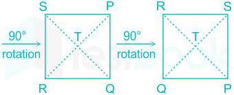
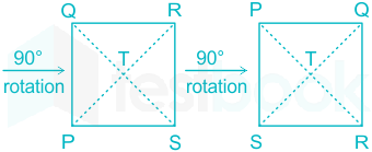
Consider the following square with the four corners and the center marked as P, Q, R, S and T respectively.

Let X, Y and Z represent the following operations:

X: rotation of the square by 180 degree with respect to the S-Q axis.

Y: rotation of the square by 180 degree with respect to the P-R axis.

Z: rotation of the square by 90 degree clockwise with respect to the axis perpendicular, going into the screen and passing through the point T.

Consider the following three distinct sequences of operation (which are applied in the left to right order).

(1) XYZZ

(2) XY

(3) ZZZZ

Which one of the following statements is correct as per the information provided above?

  1. ((a))

    The sequence of operations (1) and (2) are equivalent

  2. ((b))

    The sequence of operations (1) and (3) are equivalent

  3. ((c))

    The sequence of operations (2) and (3) are equivalent

  4. ((d))

    The sequence of operations (1), (2) and (3) are equivalent

Show Answer
Answer: ((b))

The sequence of operations (1) and (3) are equivalent

  1. For XYZZ

and ZZ

  1. XY

  1. ZZZZ

Electronics and Communication Engineering (55 questions)

11

Consider the two-dimensional vector field F(x,y)=xi+yj\vec F(x,y)=x\vec i+y \vec j, where i\vec i and j\vec j denote the unit vectors along the x-axis and the y-axis, respectively. A contour 𝐶 in the x - y plane, as shown in the figure, is composed of two horizontal lines connected at the two ends by two semicircular arcs of unit radius. The contour is traversed in the counter-clockwise sense. The value of the closed path integral

CF(x,y).(dx i+dy j)\oint_C \vec F(x,y).(dx\ \vec i+dy\ \vec j)

is ________.

  1. ((a))

    0

  2. ((b))

    1

  3. ((c))

    8 + 2π

  4. ((d))

    -1

Show Answer
Answer: ((a))

0

Concept:

Green theorem:

(Mdx+Ndy)=R(NxMy)dxdy\oint (Mdx+Ndy)= \iint_{R}^{}\left ( \frac{\partial N}{\partial x}-\frac{\partial M}{\partial y} \right )dxdy

Where the path of integration along with C is anticlockwise. 

Calculation:

CF(x,y).(dx i+dy j) \oint_C \vec F(x,y).(dx\ \vec i+dy\ \vec j) \space

Given 

F(x,y)=xi+yj \vec F(x,y)=x\vec i+y \vec j \space

CF(x,y).(dx i+dy j) =C(x i+y j).(dx i+dy j) \oint_C \vec F(x,y).(dx\ \vec i+dy\ \vec j) \space = \oint_C (x\ \vec i+y\ \vec j).(dx\ \vec i+dy\ \vec j) \space

CF(x,y).(dx i+dy j) =C(xdx+ydy) \oint_C \vec F(x,y).(dx\ \vec i+dy\ \vec j) \space = \oint_C (xdx+ydy) \space

By Green's theorem

C(xdx+ydy) =syxxy =0 \oint_C (xdx+ydy) \space = \iint_s {\dfrac{\partial y}{\partial x}-\dfrac{\partial x}{ \partial y}} \space =0\space

12

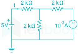
The current I in the circuit shown is ________.

  1. ((a))

    1.25 × 10-3 A

  2. ((b))

    0.75 × 10⁻³ A

  3. ((c))

    -0.5 × 10⁻³ A

  4. ((d))

    1.16 × 10⁻³ A

Show Answer
Answer: ((b))

0.75 × 10⁻³ A

  Applying KCL at junction we get current through middle branch

= (I + 10-3)A

Applying KVL we get

5 = (2K)I + 2K(I + 10-3)

5 = 2000 I + 2000 I + 2

solving for I we get

I = 0.75 × 10-3 A

13

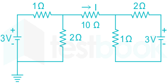
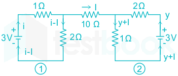
Consider the circuit shown in the figure. The current I flowing through the 10 Ω resistor is _________.

  1. ((a))

    1 A

  2. ((b))

    0 A

  3. ((c))

    0.1 A

  4. ((d))

    -0.1 A

Show Answer
Answer: ((b))

0 A

Concept: 

The current leaving a current/voltage source must be equal to current entering the source in order to justify the law of conservation of charge.

∴ For loop 2:

y = y + I

I = 0

Similarly, for Loop 1:

i = i - I

I = 0

∴ The current 'I' though resister 10 Ω will be:

I = 0 A

14

The Fourier transform X(jω) of the signal

x(t)=t(1+t2)2\rm x(t)=\frac{t}{(1+t^2)^2}

is _______.

  1. ((a))

    π2jωeω\frac{\pi}{2j}\omega e^{-|\omega|}

  2. ((b))

    π2ωeω\frac{\pi}{2}\omega e^{-|\omega|}

  3. ((c))

    π2jeω\frac{\pi}{2j} e^{-|\omega|}

  4. ((d))

    π2eω\frac{\pi}{2}e^{-|\omega|}

Show Answer
Answer: ((a))

π2jωeω\frac{\pi}{2j}\omega e^{-|\omega|}

Concept:

Let us assume the Fourier transform of x(t) is X(ω)

then as per property of duality,

x(t) \rightleftharpoons X(ω)

X(t) \rightleftharpoons 2π x(-ω)

Calculation:

We know that,

eatu(t)FT1a+jω eatu(t)FT2aa2+ω2\begin{aligned} &e^{-a t} u(t) \stackrel{F \cdot T \cdot}{\rightleftharpoons} \frac{1}{a+j ω} \ &e^{-a|t|} u(t) \stackrel{F T}{\rightleftharpoons} \frac{2 a}{a^{2}+ω^{2}} \end{aligned}

for, a = 1

e-|t| FT\stackrel{F \cdot T \cdot}{\rightleftharpoons} 21+ω2\frac{2}{1+ω^2}      ....(1)

applying differentiation in frequency property,

x(t) \rightleftharpoons X(ω)

Now,

t x(t) \rightleftharpoons j ddωX(ω)\rm \frac{d}{dω}X(ω)

tetu(t)(j)ddω[21+ω2]\rm te^{-|t|}u(t)\rightleftharpoons(j)\frac{d}{dω}\left[\frac{2}{1+ω^2}\right]

tetu(t)4jω(1+ω2)2\rm te^{-|t|}u(t)\rightleftharpoons\frac{-4jω}{(1+ω^2)^2}       .....(2)

applying property of duality in eqn (2) we get,

tetu(t)4jω(1+ω2)2\rm te^{-|t|}u(t)\rightleftharpoons\frac{-4jω}{(1+ω^2)^2}

t = -ω

4jt(1+t2)22πωeω\frac{-4jt}{(1+t^2)^2}\rightleftharpoons-2\pi \omega e^{-|\omega|}

t(1+t2)2π2jωeω\frac{t}{(1+t^2)^2}\rightleftharpoons\frac{\pi}{2j} \omega e^{-|\omega|}

15

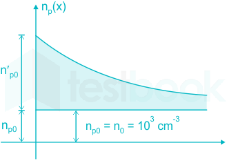
Consider a long rectangular bar of direct bandgap p-type semiconductor. The equilibrium hole density is 1017 cm-3 and the intrinsic carrier concentration is 1010 cm-3 . Electron and hole diffusion lengths are 2 μm and 1 μm, respectively.

The left side of the bar (x = 0) is uniformly illuminated with a laser having photon energy greater than the bandgap of the semiconductor. Excess electron-hole pairs are generated ONLY at x = 0 because of the laser. The steady state electron density at x = 0 is 1014 cm-3 due to laser illumination. Under these conditions and ignoring electric field, the closest approximation (among the given options) of the steady state electron density at x = 2 μm, is ___________ .

  1. ((a))

    0.37 × 1014 cm-3

  2. ((b))

    0.63 × 1013 cm-3

  3. ((c))

    3.7 × 1014 cm-3

  4. ((d))

    103 cm-3

Show Answer
Answer: ((a))

0.37 × 1014 cm-3

Concept:

Extrinsic p-type semiconductors are formed when a trivalent impurity is added to a pure semiconductor. Examples of trivalent impurity are Boron, Gallium, and Indium.

Also, the law of mass action is used to determine the minority carriers in a doped semiconductor.

According to law:

n0.p0 = ni2

n0 = concentration of electrons

p0 = concentration of holes

For a steady-state carrier injection, the excess carrier concentration dies out exponentially for a distance ‘x’ due to recombination.

Mathematically this is defined as:

δp(x) = δp(0) e-x/Lp

δn(x) = δn(0) e-x/Ln

Ln and Lp are the diffusion length of electrons and holes respectively.

Calculation:

Given, P = 1017 cm-3 = P0

n0=ni2P0=10201017=103 cm3\rm n_{0}=\frac{n_{i}^{2}}{P_{0}}=\frac{10^{20}}{10^{17}}=10^{3} \mathrm{~cm}^{-3}

Ln = 2 μm

n'PO = 1014 cm-3

Excess electron concentration at any distance x is

δnp(x) = n'P0 e-x/Ln

= 1014 e-2/2

= 1014 e-1

= 3.67 × 1013 cm-3

= 0.367 × 1014 cm-3

16

Consider an even polynomial p(s) given by

p(s) = s4 + 5s2 + 4 + K

where K is an unknown real parameter. The complete range of K for which p(s) has all its roots on the imaginary axis is ________.

  1. ((a))

    4K94 -4 \le K \le\frac{9}{4} \space

  2. ((b))

    3K92 -3 \le K \le\frac{9}{2}\space

  3. ((c))

    6K54 -6 \le K \le\frac{5}{4}\space

  4. ((d))

    5K0 -5 \le K \le 0\space

Show Answer
Answer: ((a))

4K94 -4 \le K \le\frac{9}{4} \space

Calculation:

P(s) = s4 + 5s2 + (4 + K)

Given: p(s) = s4 + 5s2 + (4 + K)

Routh's Table:

s415(4+K) s300 s2 s1 s0\begin{array}{c|ccc} s^{4} & 1 & 5 & (4+K) \ s^{3} & 0 & 0 \ s^{2} && \ s^{1} & & & \ s^{0} & & & \end{array}

As all row of s3 are zero,

A(s) = s4 + 5s2 + (4 + K)

s415(4+K) s34100 s210452(4+K) s1254(4+K)5/2 s04+K\begin{array}{c|ccc} s^{4} & 1 & 5 & (4+K) \ s^{3} & 4 & 10 & 0 \ s^{2} & \frac{10}{4}-\frac{5}{2} & (4+K) & \ s^{1} & \frac{25-4(4+K)}{5 / 2} & & \ s^{0} & 4+K & & \end{array}

1st column of R-H table must be all positive.

i.e., 254(4+K)5/2>0K<94\frac{25-4(4 + K)}{5/2} > 0 ⇒ K < \frac{9}{4}

4 + K > 0 ⇒ K > -4

Range of K: 4<K<94-4 < K < \frac{9}{4}

17

In a non-degenerate bulk semiconductor with electron density n = 1016 cm-3 , the value of EC - EFn = 200 meV, where EC and EFn denote the bottom of the conduction band energy and electron Fermi level energy, respectively. Assume thermal voltage as 26 meV and the intrinsic carrier concentration is 1010 cm-3 . For n = 0.5 × 1016 cm-3 , the closest approximation of the value of (EC − EFn), among the given options, is __________.

  1. ((a))

    226 meV

  2. ((b))

    174 meV

  3. ((c))

    218 meV

  4. ((d))

    182 meV

Show Answer
Answer: ((c))

218 meV

Concept:

Fermi level in n-type Semiconductor:

The position of the Fermi level in the n-type semiconductor is given as:

EF=ECKTln[NCND] {E_F} = {E_C} -KT\ln \left[ {\frac{{{N_C}}}{{{N_D}}}} \right]

Fermi level in p-type Semiconductor:

The position of the Fermi level in the p-type semiconductor is given as:

EF=EVKTln[NVNA] {E_F} ={E_V} - KT\ln \left[ {\frac{{{N_V}}}{{{N_A}}}} \right]

Calculation:

Given:

ND1 = 1016 cm-3

ND2 = 0.5 × 1016 cm-3

\(\rm (E_{C}-E_{F n}){1}=k T \ln \left(\frac{N{C}}{N_{D 1}} \right)=200 \) meV

\(\rm (E_{C}-E_{F n}){2}=k T \ln \left(\frac{N{C}}{N_{D 2}} \right)\)

\(\rm \left(E_{C}-E_{F n}\right){1}-\left(E{C}-E_{F n}\right){2}=k T \ln \left(\frac{N{C}}{N_{D 1}}\right)-k T \ln \left(\frac{N_{C}}{N_{D 2}}\right)\)

\(\rm 200 \ meV -\rm (E_{C}-E_{F n}){2}=k T \ln \left(\frac{N{D2}}{N_{D 1}} \right)\)

200 meV(ECEFn)2=0.026ln(1016×0.51016)\rm 200 \ meV -\rm (E_{C}-E_{F n})_{2}=0.026 \ln \left( \frac{10^{16} \times 0.5}{10^{16}} \right)

200 meV(ECEFn)2\rm 200 \ meV -\rm (E_{C}-E_{F n})_{2} = 0.026 ln(0.5)

200 meV(ECEFn)2\rm 200 \ meV -\rm (E_{C}-E_{F n})_{2} = -0.01802 volt

200 meV(ECEFn)2\rm 200 \ meV -\rm (E_{C}-E_{F n})_{2} = -18.02 meV

(EC - EFn)2 = 200 meV + 18.02 meV

= 218.02 meV

18

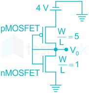
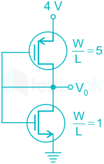
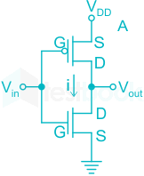
Consider the CMOS circuit shown in the figure (substrates are connected to their respective sources). The gate width (W) to gate length (L) ratios (WL)\left(\frac{W}{L}\right) of the transistors are as shown. Both the transistors have the same gate oxide capacitance per unit area. For the pMOSFET, the threshold voltage is -1 V and the mobility of holes is 40 cm2V.s\rm \frac{cm^2}{V.s}. For the nMOSFET, the threshold voltage is 1 V and the mobility of electrons is 300 cm2V.s\rm \frac{cm^2}{V.s} The steady state output voltage V0 is _________.

  1. ((a))

    equal to 0 V

  2. ((b))

    more than 2 V

  3. ((c))

    less than 2 V

  4. ((d))

    equal to 2 V

Show Answer
Answer: ((c))

less than 2 V

Concept:

MOSFET is in saturation region:

VGS > Vth

VDS > VGS – Vth

The current equation for a MOSFET in the saturation region is given by:

\({{I}{D}}=\frac{1}{2}{{\mu }{n}}{{C}{OX}}\frac{W}{L}{{\left( {{V}{GS}}-{{V}_{th}} \right)}^{2}}\)

\({{I}{D}}=\frac{K_n}{2}{{\left( {{V}{GS}}-{{V}_{th}} \right)}^{2}}\)

Calculation:

Both MOSFETs are in saturation because drain is shorted to Gate.

IDSN = ISDP

\(\frac{\mu_{n} C_{o x}}{2} ×\left(\frac{W}{L}\right){N}\left(V{G S N}-V_{T N}\right)^{2}=\frac{\mu_{p} C_{o x}}{2}\left(\frac{W}{L}\right){P}\left(V{S G P}-\left|V_{T P}\right|\right)^{2}\)

300 × 1 (V0 - 1)2 = 40 × 5(4 - V0 - 1)2

3(V02+12V0)=2(9+V026V0)3(V_0^2 + 1 - 2V_0) = 2(9 + V_0^2 - 6 V_0)

⇒ V02+6V015=0V_0^2 + 6V_0 - 15 = 0

V0=6±36+4×152=6±962V_0 = \frac{-6 \pm \sqrt{36 + 4 \times 15}}{2} = \frac{-6 \pm \sqrt{96}}{2}

V0 = 1.898 V, -7.89 V

V0 cannot be negative because V0 should lie between 0 and 4 V.

V0 = 1.898 V (Less than 2V)

19

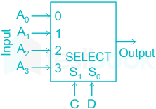
Consider the 2-bit multiplexer (MUX) shown in the figure. For OUTPUT to be the XOR of C and D, the values for A0, A1, A2, and A3 are ________.

  1. ((a))

    A0 = 0, A1 = 0, A2 = 1, A3 = 1

  2. ((b))

    A0 = 1, A1 = 0, A2 = 1, A3 = 0

  3. ((c))

    A0 = 0, A1 = 1, A2 = 1, A3 = 0

  4. ((d))

    A0 = 1, A1 = 1, A2 = 0, A3 = 0

Show Answer
Answer: ((c))

A0 = 0, A1 = 1, A2 = 1, A3 = 0

The correct answer is option 3.

Concept:

The multiplexer abbreviated "MUX" or "MPX," is a combinational logic circuit that uses a control signal to switch one of the numerous input lines to a single common output line.

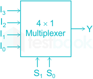
S1, S0 are the select lines, I1, I2, I3, and I4 are the input lines and produce the output Y.

Digital Circuits - Multiplexers

Y= (S1' S0' )I0+( S1'S0 )I1+(S1 S0' )I2 +( S1S0 )I3


Explanation:

Option 1: A0 = 0, A1 = 0, A2 = 1, A3 = 1

These input lines A0 = 1, A1 = 0, A2 = 1, A3 = 0, C and D are the select lines and produce the output 

Y= (C' D' ) 0+( C' D ) 0+(C D' ) 1+( CD) 1

Y=0+0+CD'+CD

Y=C(D'+D)

Y=C

Option 2: A0 = 1, A1 = 0, A2 = 1, A3 = 0

These input lines A0 = 0, A1 = 0, A2 = 1, A3 = 1, C and D are the select lines and produce the output 

Y= (C'D') 1+( C' D ) 0+(C D' ) 1+( CD) 0

Y= C'D'+0+CD'+0

Y=D'(C'+C)

Y=D'

Option 3: A0 = 0, A1 = 1, A2 = 1, A3 = 0

These input lines A0 = 0, A1 = 1, A2 = 1, A3 = 0, C and D are the select lines and produce the output 

Y= (C'D') 0+( C' D) 1+(CD') 1+( CD) 0

Y= 0 + C'D + CD' + 0

Y=C'D + CD'

Option 4: A0 = 1, A1 = 1, A2 = 0, A3 = 0

These input lines A0 = 1, A1 = 1, A2 = 0, A3 = 0, C and D are the select lines and produce the output 

Y= (C'D') 1 + ( C' D ) 1 + (C D' ) 0 + ( CD) 0

Y= C'D '+ C'D + 0 + 0

Y=C'D '+ C'D

Y=C'(D' + D)

Y = C'

Hence the correct answer is A0 = 0, A1 = 1, A2 = 1, A3 = 0.

20

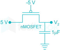
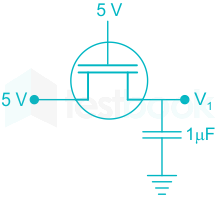
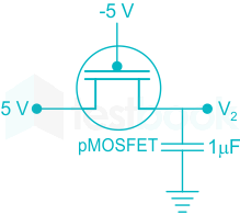
The ideal long channel nMOSFET and pMOSFET devices shown in the circuits have threshold voltages of 1 V and -1 V, respectively. The MOSFET substrates are connected to their respective sources. Ignore leakage currents and assume that the capacitors are initially discharged. For the applied voltages as shown, the steady-state voltages are ___________.


  1. ((a))

    V1 = 5 V, V2 = 5 V

  2. ((b))

    V1 = 5 V, V2​ = 4 V

  3. ((c))

    V1 = 4 V, V2​ = 5 V

  4. ((d))

    V1 = 4 V, V2​ = -5 V

Show Answer
Answer: ((c))

V1 = 4 V, V2​ = 5 V

Vc1 = min(VG - VT, VD)

= min(4, 5)

Vc1 = 4V


VSG  > |VTP|

VC2 + 4 > 1

VC2 > -4

VSD > 0

VC2 > 5V

VC2 = 5V

21

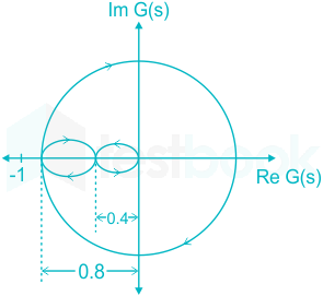
Consider a closed-loop control system with unity negative feedback and KG(s) in the forward path, where the gain K = 2. The complete Nyquist plot of the transfer function G(s) is shown in the figure. Note that the Nyquist contour has been chosen to have the clockwise sense. Assume G(s) has no poles on the closed right-half of the complex plane. The number of poles of the closed-loop transfer function in the closed right-half of the complex plane is ___________.

  1. ((a))

    0

  2. ((b))

    1

  3. ((c))

    2

  4. ((d))

    3

Show Answer
Answer: ((c))

2

Concept:

Nyquist stability criterion:

N = P – Z

N is the number of encirclements of (-1+j0) point by the Nyquist contour in an anticlockwise direction.

P is the open-loop RHP poles

Z is the closed-loop RHP poles

Analysis:

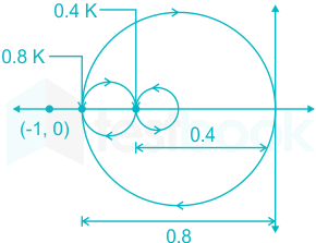
For K = 1,

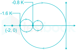
For K = 2, the plot will be

N = No. of encirclement about (-1, 0) in anticlockwise.

P = Total number of open loop poles, in R.H.S.

Z = P - N

N = -2, P = 0

Z = 0 - (-2) = 2

Z = 2

Two poles in right side.

22

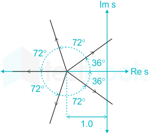
The root-locus plot of a closed-loop system with unity negative feedback and transfer function KG(s) in the forward path is shown in the figure. Note that K is varied from 0 to ∞.

Select the transfer function G(s) that results in the root-locus plot of the closed-loop system as shown in the figure.

  1. ((a))

    G(s)=1(s+1)5\rm G(s)=\frac{1}{(s+1)^5}

  2. ((b))

    G(s)=1s5+1\rm G(s)=\frac{1}{s^5+1}

  3. ((c))

    G(s)=s1(s+1)6\rm G(s)=\frac{s-1}{(s+1)^6}

  4. ((d))

    G(s)=s+1s6+1\rm G(s)=\frac{s+1}{s^6+1}

Show Answer
Answer: ((a))

G(s)=1(s+1)5\rm G(s)=\frac{1}{(s+1)^5}

Concept:

The number of branches of the root locus diagram is:

N = P if P ≥ Z

= Z, if P ≤ Z

Application:

Here 5 Root Locus branches are diverging from the same point, this can possible only when if we have 5 poles in the system at the same point because the Root Locus branch departs from the open-loop pole and

The Number of Root Locus branches = Number of open-loop poles or Number of zero (Whichever is greater).

Here, there are 5 multiple Real poles, matching with option (A). 

So, correct option is 1(s+1)5\frac{1}{(s + 1)^5}

Additional Information

  1. Every branch of a root locus diagram starts at a pole (K = 0) and terminates at a zero (K = ∞) of the open-loop transfer function.
  2. The root locus diagram is symmetrical with respect to the real axis.
  3. The number of branches of the root locus diagram are:

N = P if P ≥ Z

= Z, if P ≤ Z

4. Number of asymptotes in a root locus diagram = |P – Z| 5. Centroid: It is the intersection of the asymptotes and always lies on the real axis. It is denoted by σ.

σ=PiZiPZ\sigma = \frac{{\sum {P_i} - \sum {Z_i}}}{{\left| {P - Z} \right|}}

ΣPi is the sum of real parts of finite poles of G(s)H(s)

ΣZi is the sum of real parts of finite zeros of G(s)H(s)

6. Angle of asymptotes: 

l = 0, 1, 2, … |P – Z| – 1

7. On the real axis to the right side of any section, if the sum of a total number of poles and zeros are odd, the root locus diagram exists in that section.​

23

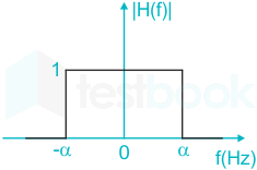
The frequency response H(f) of a linear time-invariant system has magnitude as shown in the figure.

Statement I: The system is necessarily a pure delay system for inputs which are bandlimited to −α ≤ f ≤ α.

Statement II: For any wide-sense stationary input process with power spectral density SX(f), the output power spectral density 𝑆Y(f) obeys SY(f) = SX(f) for −α ≤ f ≤ α. Which one of the following combinations is true?

  1. ((a))

    Statement I is correct, Statement II is correct

  2. ((b))

    Statement I is correct, Statement II is incorrect

  3. ((c))

    Statement I is incorrect, Statement II is correct

  4. ((d))

    Statement I is incorrect, Statement II is incorrect

Show Answer
Answer: ((a))

Statement I is correct, Statement II is correct

Analysis(1):

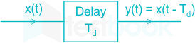
Let x(t) signal is delayed by time Td. If y(t) is the response of delayed system-

y(t) = x(t-Td) ..............(1)

Let take the Fourier transform of equation (1)

Y(f) = X(f).e2jπfTde^{-2j\pi fT_d}

H(f) = Y(f)/X(f)=e2jπfTdY(f)/X(f) = e^{-2j\pi fT_d}

| H(f) | = 1 and

H(f)=2jπfTd\angle H(f) ={-2j\pi fT_d}

It shows that system has magnitude 1 and system is bandlimited to −α ≤ f ≤ α, hence statement 1 is correct.

Analysis(2):

For a wide-sense stationary input process:

Power spectral density (PSD)o = SX(f)

Output power spectral density (PSD)i = 𝑆Y(f) 

\(\begin{aligned} (\mathrm{PSD}){o} &=(\mathrm{PSD}){i} \cdot|H(f)|^{2} \ \end{aligned}\)

SY(f)=SX(f);αfα \begin{aligned} S_{Y}(f) &=S_{X}(f) \quad ; \quad-\alpha \leq f \leq \alpha \ \end{aligned}

Phase response of the system is not given, hence statement 2 is correct.

24

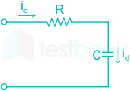
In a circuit, there is a series connection of an ideal resistor and an ideal capacitor. The conduction current (in Amperes) through the resistor is 2 sin(t + π/2). The displacement current (in Amperes) through the capacitor is _________

  1. ((a))

    2 sin (t)

  2. ((b))

    2 sin (t + π)

  3. ((c))

    2 sin (t + π/2)

  4. ((d))

    0

Show Answer
Answer: ((c))

2 sin (t + π/2)

Concept:

Conduction current density:

  • Conduction current comes from the movement of charges such as electrons present in conductors or and semiconductors.
  • The electrons present in the conduction band of conductors or semiconductors are free and they respond to the applied electric field.
  • The current passing through due to such free election per unit cross-sectional area per unit time is commonly referred to as conduction current density.


Jc=IcA=σE(Ampm2){J_c} = \frac{{{I_c}}}{A} = \sigma E\left( {\frac{{Amp}}{{{m^2}}}} \right)

Displacement current density:

  • Displacement current comes from the change in the electric field caused by the displacement of the center of positive charge and center of negative charge of a dielectric or insulating medium.
  • Dielectric does not contain free electrons for conduction, rather they contain immobile charges and are displaced slightly from their equilibrium position in the presence of the electric field.
  • Consequently, they produce a change in the electric field present in the dielectric medium and hence displacement current.
  • The rate of change of such electric field with respect to time is commonly referred to as displacement current density.


JD=JDA=μtA=t(ψA)=Dt{J_D} = \frac{{{J_D}}}{A} = \frac{{\frac{{\partial \mu }}{{\partial t}}}}{A} = \frac{\partial }{{\partial t}}\left( {\frac{\psi }{A}} \right) = \frac{{\partial D}}{{\partial t}}

JD=Dt=ωD=2πfεoεrE{J_D} = \frac{{\partial D}}{{\partial t}} = \omega D = 2\pi f{\varepsilon _o}{\varepsilon _r}E

Analysis:

In a series connection, the current through each element remains the same, Hence ic = id

id=2sin(t+π2)\rm i_d = 2 \sin \left( t + \frac{\pi}{2} \right)

25

Consider an FM broadcast that employs the pre-emphasis filter with frequency response

Hpe(ω)=1+jωω0\rm H_{pe}(ω)=1+\frac{jω}{ω_0}

where ω0 = 104 rad/sec.

For the network shown in the figure to act as a corresponding de-emphasis filter, the appropriate pair(s) of (R, C) values is/are ________.

  1. ((a))

    R = 1 kΩ, C = 0.1 μF

  2. ((b))

    R = 2 kΩ, C = 1 μF

  3. ((c))

    R = 1 kΩ, C = 2 μF

  4. ((d))

    R = 2 kΩ, C = 0.5 μF

Show Answer
Answer: ((a))

R = 1 kΩ, C = 0.1 μF

Concept:

Relationship between de-emphasis filter and pre-emphasis filter is-

Hpe(ω)=1Hde(ω)\left|H_{p e}(ω)\right|=\frac{1}{\left|H_{d e}(ω)\right|}

Where,

Hpe(ω) - Frequency response of pre-emphasis filter

Hde(ω) - Frequency response of de-emphasis filter

Given:

Frequency response of pre-emphasis filter-

Hpe(ω)=1+jωω0\rm H_{pe}(ω)=1+\frac{jω}{ω_0}

ω0 = 104 rad/sec

and

de-emphasis filter

Solution:

Hpe(ω)=1Hde(ω)\left|H_{p e}(\omega)\right|=\frac{1}{\left|H_{d e}(\omega)\right|}

Hpe(ω)2=1Hde(ω)2\left|H_{p e}(\omega)\right|^{2}=\frac{1}{\left|H_{d e}(\omega)\right|^{2}}

So,

1+(ωω0)2=1+(ωRC)21+\left(\frac{\omega}{\omega_{0}}\right)^{2}=1+(\omega R C)^{2}

1ω0=RC\frac{1}{\omega_{0}}=R C

RC = 10-4

Only Option (1) satisfies the above condition.

Hence option (1) is correct.

26

Consider the following partial differential equation (PDE)

a2f(x,y)x2+b2f(x,y)y2=f(x,y)\rm a\frac{\partial^2f(x,y)}{\partial x^2}+b\frac{\partial^2f(x,y)}{\partial y^2}=f(x,y)

where a and b are distinct positive real numbers. Select the combination(s) of values of the real parameters 𝜉 and 𝜂 such that f(x, y) = e(ξx + ny) is a solution of the given PDF.

  1. ((a))

    ξ=12a,η=12b\xi=\frac{1}{\sqrt{2a}}, \eta=\frac{1}{\sqrt{2b}}​​​

  2. ((b))

    ξ=1a,η=0\xi=\frac{1}{\sqrt{a}}, \eta=0

  3. ((c))

    ξ = 0, η = 0

  4. ((d))

    ξ=1a,η=1b\xi=\frac{1}{\sqrt{a}}, \eta=\frac{1}{\sqrt{b}}

Show Answer
Answer: ((a))

ξ=12a,η=12b\xi=\frac{1}{\sqrt{2a}}, \eta=\frac{1}{\sqrt{2b}}​​​

Analysis:

Given

f(x, y) = e(ξ x + n y)

2f(x,y)x2=ξ2 f(x,y) \frac{\partial^2f(x,y)}{\partial x^2}=ξ ^2\space f(x,y)\space  →  (1)

2f(x,y)y2=n2 f(x,y) \frac{\partial^2f(x,y)}{\partial y^2}=n^2\space f(x,y)\space  → (2)

By the given partial equation and equation 1 and 2 

a ξ 2 f(x, y) + b n2 f(x, y) = f(x, y)

a ξ 2  + b n2  = 1

Now go by options

From option 1

ξ=12a,η=12b ξ=\frac{1}{\sqrt{2a}}, \eta=\frac{1}{\sqrt{2b}} \space

a ξ 2  + b n2  = 1   ⇒  a × (1/2a) + b (1/2b)  = 1      (Option 1 is correct)

From option 2 

ξ=1a,η=0 ξ=\frac{1}{\sqrt{a}}, \eta=0 \space

a ξ 2  + b n2  = 1  ⇒  a × (1/a) + 0 = 1    (Option 2 is correct)

From option 3

ξ = 0, η = 0

a ξ 2  + b n2  = 1  ⇒  a × (0) + 0 = 1   

a ξ 2  + b n2  ≠ 1        (Option 3  is incorrect)

From option 4

ξ=1a,η=1b \xi=\frac{1}{\sqrt{a}}, \eta=\frac{1}{\sqrt{b}} \space

a ξ 2  + b n2  = 1  ⇒  a × (1/a) + b× (1/b) =  2 

a ξ 2  + b n2  ≠ 1        (Option 4  is incorrect)

27

Consider communication over a memoryless binary symmetric channel using a (7, 4) Hamming code. Each transmitted bit is received correctly with probability(1 -ϵ), and flipped with probability ϵ. For each codeword transmission, the receiver performs minimum Hamming distance decoding, and correctly decodes the message bits if and only if the channel introduces at most one bit error.

For ϵ = 0.1, the probability that a transmitted codeword is decoded correctly is _________ (rounded off to two decimal places).

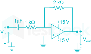
28

An ideal OPAMP circuit with a sinusoidal input is shown in the figure. The 3 dB frequency is the frequency at which the magnitude of the voltage gain decreases by 3 dB from the maximum value. Which of the options is/are correct?

  1. ((a))

    The circuit is a low pass filter.

  2. ((b))

    The circuit is a high pass filter.

  3. ((c))

    The 3 dB frequency is 1000 rad/s.

  4. ((d))

    The 3 dB frequency is 10003\frac{1000}{3} rad/s

Show Answer
Answer: ((a))

The circuit is a low pass filter.

The given op-amp is inverting type, hence the gain is given as:

VoVin=20001000+1jω×106\frac{V_o}{V_{in}}=-\frac{2000}{1000+\frac{1}{jω\times10^{-6}}}

V0Vin=21+1jω1000\frac{V_0}{V_{in}}=\frac{-2}{1+\frac{1}{\frac{jω}{1000}}}

At ω = ∞

Gain=V0Vin=2Gain=\frac{V_0}{V_{in}}=-2

At ω = 0

Gain=V0Vin=0Gain=\frac{V_0}{V_{in}}=0

Hence the given op-amp is High Pass Filter.

Now, the  3 dB Cut-off frequency is given as:

ωc=1R1C1=1103×106ω_c = \frac{1}{R_1 C_1} = \frac{1}{10^3 \times 10^{-6} }

ωc = 1000 rad/sec

Hence, option (b) and (c) is correct.

29

Select the Boolean function(s) equivalent to x + yz, where x, y, and z are Boolean variables, and + denotes logical OR operation.

  1. ((a))

    x + z + xy

  2. ((b))

    (x + y)(x + z)

  3. ((c))

    x + xy + yz

  4. ((d))

    x + xz + xy

Show Answer
Answer: ((a))

x + z + xy

The correct answer is option 2 and option 3.

Concept:

Boolean function:

The variables used in Boolean Algebra only have one of two possible values, a logic “0” and a logic “1” but an expression can have an infinite number of variables all labeled individually to represent inputs to the expression.

For example, variables A, B, C, etc, give us a logical expression of A + B = C, but each variable can ONLY be a 0 or a 1.

Explanation:

The given expression is = x + yz the equivalent expression is,

Option 1:  x + z + xy

= x + z + xy

= x(1+y)+ z  (∴ 1 + x = x + 1 = 1)

= x + z it is not equivalent x + yz.

Option 2:  (x + y)(x + z)

= (x + y)(x + z)

=x + xz + yx + yz

=x(1+ z+ y) + yz  (∴1 + x = x + 1 = 1)

= x + yz it is equivalent x + yz.

Option 3:  x + xy + yz

= x + xy + yz

= x(1 + y) +yz

= x + yz  it is equivalent x + yz.

Option 4:  x + xz + xy

= x + xz + xy

= x(1+z+y) (∴1 + x = x + 1 = 1)

= x it is not equivalent x + yz.

Hence the correct answer is option 2 and option 3.

30

Select the correct statement(s) regarding CMOS implementation of NOT gates.

  1. ((a))

    Noise Margin High (NMH) is always equal to the Noise Margin Low (NML), irrespective of the sizing of transistors.

  2. ((b))

    Dynamic power consumption during switching is zero.

  3. ((c))

    For a logical high input under steady state, the nMOSFET is in the linear regime of operation.

  4. ((d))

    Mobility of electrons never influences the switching speed of the NOT gate.

Show Answer
Answer: ((c))

For a logical high input under steady state, the nMOSFET is in the linear regime of operation.

Correct answer is option (3)

Explanation:

Option (1):

  • Noise is an undesirable signal that is superimposed upon the normal operating signal.
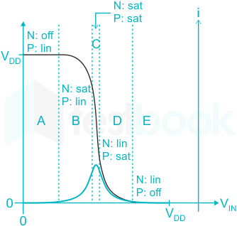
  • Noise margin the maximum tolerable noise voltage that can be added so that the circuit that does not cause an undesirable change in the circuit 's output.
       

NML = VIL - VOL 

NMH = VOH - VIH

If the size of both transistors ( pMOS and nMOS) are equal

Under the condition:

VTN = VTP

Kn = KP 

Vin VDD2\frac{V_{DD}}{2}

in such case : NML = NMH 

If the size of both transistor are unequal, then KNKPK_{N}\neq K_{P}

When ; KpKN>1,than VIL,VIH\uparrow \frac{K_{p}}{K_{N}}>1, \text{than } V_{IL}\uparrow, V_{IH}\downarrow

NMH\downarrow and NMLN_{ML}\uparrow

Now,

When ; KpKN<1,than VIL,VIH\uparrow \frac{K_{p}}{K_{N}}<1, \text{than } V_{IL}\downarrow, V_{IH}\uparrow

NMHandNMLN_{MH}\uparrow and \quad N_{ML}\downarrow

Hence, option (1) is incorrect.

Option (2):

Dynamic power consumption during switching is non zero due to capacitive loading of next stage.

Hence, option(2) is incorrect.

Option (3):


Logic High input: VDDVTP<Vin<VDDV_{DD}- |V_{TP}|<V_{in}<V_{DD}

In this region : pMOS → Cutoff 

nMOS → Linear 

Hence, option (3) is correct.

Option (4)

  • For fast charging and discharging capacitor depends upon the mobility of the charge carrier.
  • Mobility influences the switching speed of the NOT gate.

Hence, option (4) is incorrect.

31

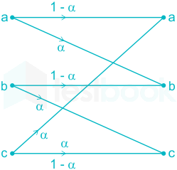
The transition diagram of a discrete memoryless channel with three input symbols and three output symbols is shown in the figure. The transition probabilities are as marked.

The parameter α lies in the interval [0.25, 1]. The value of α for which the capacity of this channel is maximized, is ________ (rounded off to two decimal places).

32

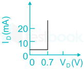
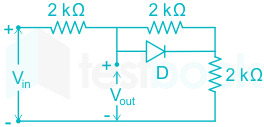
A circuit and the characteristics of the diode (D) in it are shown. The ratio of the minimum to the maximum small signal voltage gain VoutVin\frac{\partial V_{out}}{\partial V_{in}} is _______(rounded off to two decimal places).

33

Let H(X) denote the entropy of a discrete random variable X taking K possible distinct real values. Which of the following statements is/are necessarily true?

  1. ((a))

    H(X) ≤ log2 K bits

  2. ((b))

    H(X) ≤ H(2X)

  3. ((c))

    H(X) ≤ H(X2)

  4. ((d))

    H(X) ≤ H(2X)

Show Answer
Answer: ((a))

H(X) ≤ log2 K bits

Given:

X is a discrete random variable , K possible distinct real values.

Analysis:

If 'K' symbols having equal probability:

Maximum Entropy  H(X)max = log2 (K).

If 'K' symbols having different probabilities:

H(X) < log2 (K)

So, H(X) ≤ log2 (K) Option (1) is correct.

As per given option (2):

H(X) ≤ H(2X)

\(\begin{aligned} &\begin{array}{|c|ccc|} \hline X \in\left{x_{i}\right} & -1 & 0 & 1 \ \hline P_{X}\left(x_{i}\right) & \frac{1}{4} & \frac{1}{2} & \frac{1}{4} \ \hline \end{array}\ \end{aligned}\)

\(H(X)=\sum_{i} P_{X}\left(x_{i}\right) \log {2} \frac{1}{P{X}\left(x_{i}\right)}\)

H(f)=14log24+12log22+14log24H(f) = \frac{1}{4} \log _{2} 4+\frac{1}{2} \log _{2} 2+\frac{1}{4} \log _{2} 4

H(X)=1.5 bits  symbol H(X)=1.5 \frac{\text { bits }}{\text { symbol }}

Now , Y = 2X

XYP(Y)
-1-21/4
001/2
121/4


Xϵ{yi}-202
PY(yi)1/41/21/4


\(H(2 X)=H(Y)=\sum_{i} P_{Y}\left(y_{i}\right) \log {2} \frac{1}{P{Y}\left(y_{i}\right)}=1.5 \frac{\text { bits }}{\text { symbol }}\)

For Y = 2X, distant X values results in distinct ‘Y’ values so that H(X) = H(Y). So, option (2) is correct.

As per given option (3):

H(X) ≤ H(X2)

Now , Y = X2

\(H\left(X^{2}\right)=H(Y)=\sum_{i} P_{Y}\left(y_{i}\right) \log {2} \frac{1}{P{Y}\left(y_{i}\right)}\)

H(f)=12log22+12log22=1 bit  symbol H(f)=\frac{1}{2} \log _{2} 2+\frac{1}{2} \log _{2} 2=1 \frac{\text { bit }}{\text { symbol }}

Whereas,

H(X)=1.5 bits  symbol \mathrm{H}(\mathrm{X})=1.5 \frac{\text { bits }}{\text { symbol }}

Hence option (3) is incorrect.

As per given option (4) :

H(X) ≤ H(2X)

Now , Y = 2X

Here distinct ‘X’ values results in distinct ‘Y’ values. So that,

H(X) = H(Y) i.e. H(X) = H(2X) so, Option (4) is correct.

NOTE: Option 1, 2, 4 are correct.

34

Consider the following wave equation,

2f(x,t)t2=100002f(x,t)x2\frac{\partial^2f(x,t)}{\partial t^2}=10000\frac{\partial^2f(x,t)}{\partial x^2}

Which of the given options is/are solution(s) to the given wave equation?

  1. ((a))

    f(x,t)=e(x100t)2+e(x+100t)2f(x, t)=e^{-(x-100t)^2}+e^{-(x+100t)^2}

  2. ((b))

    f(x,t)=e(x100t)+0.5e(x+1000t)f(x, t)=e^{-(x-100t)}+0.5e^{-(x+1000t)}

  3. ((c))

    f(x,t)=e(x100t)+sin(x+100t)f(x, t)=e^{-(x-100t)}+\sin (x+100t)

  4. ((d))

    f(x,t)=ej100π(100x+t)+ej100π(100x+t)f(x, t)=e^{j100\pi(-100x+t)}+e^{j100\pi(100x+t)}

Show Answer
Answer: ((a))

f(x,t)=e(x100t)2+e(x+100t)2f(x, t)=e^{-(x-100t)^2}+e^{-(x+100t)^2}

Concept:

One dimensional wave equation:

 2ut2=C22ux2\frac{{{\partial ^2}u}}{{\partial {t^2}}} = {C^2}\frac{{{\partial ^2}u}}{{\partial {x^2}}}

Two-dimensional wave equation:

 2ut2=2ux2+2uy2\frac{{{\partial ^2}u}}{{\partial {t^2}}} = \frac{{{\partial ^2}u}}{{\partial {x^2}}} + \frac{{{\partial ^2}u}}{{\partial {y^2}}}

Analysis:

The solution is given as:

F = f(x ± ct)

option 1 and 3 satisfies the given conditions.

35

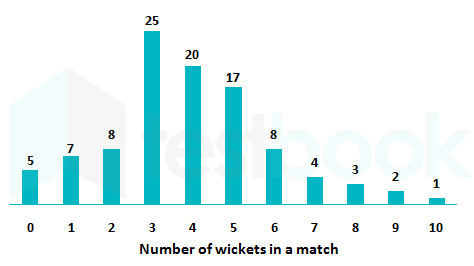
The bar graph shows the frequency of the number of wickets taken in a match by a bowler in her career. For example, in 17 of her matches, the bowler has taken 5 wickets each. The median number of wickets taken by the bowler in a match is __________ (rounded off to one decimal place).

36

A simple closed path 𝐶 in the complex plane is shown in the figure. If

2zz21dz=iπA\oint \frac{2^z}{z^2-1}dz=-i\pi A

where i = √-1 then the value of A is _______ (rounded off to two decimal places)

37

In an electrostatic field, the electric displacement density vector D is given by

D(x,y,z)=(x3i^+y3j^+xy2k^)\vec{D}(x, y,z)=(x^3 \hat{i}+y^3 \hat{j}+xy^2\hat{k}) C/m2,

Where, i^,j^, k^\hat{i}, \hat{j},\ \hat{k}  are the unit vectors along the x-axis, y-axis, and z-axis, respectively. Consider a cubical region 𝑅 centered at the origin with each side of length 1 m, and vertices at (± 0.5 m, ± 0.5 m, ± 0.5 m). The electric charge enclosed within 𝑅 is _________ C (rounded off to two decimal places).

38

Let x1(t) = e-tu(t) and x2(t) = u(t) - u(t - 2), where u(⋅) denotes the unit step function.

If y(t) denotes the convolution of x1(t) and x2(t), then limty(t)=\displaystyle \lim_{t\rightarrow\infty}y(t)= __________ (rounded off to one decimal place).

39

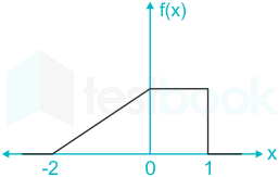
Consider a real valued source whose samples are independent and identically distributed random variables with the probability density function, f(x), as shown in the figure.

Consider a 1 bit quantizer that maps positive samples to value 𝛼 and others to value 𝛽. If α* and β* are the respective choices for α and β that minimize the mean square quantization error, then (α* - β*) = _________ (rounded off to two decimal places).

40

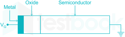
An ideal MOS capacitor (p-type semiconductor) is shown in the figure. The MOS capacitor is under strong inversion with VG = 2 V. The corresponding inversion charge density (QiN) is 2.2 μC/cm2. Assume oxide capacitance per unit area as COX = 1.7 μF/cm2. For VG = 4 V, the value of QIN is _______μC/cm2. (rounded off to one decimal place).

41

A symbol stream contains alternate QPSK and 16-QAM symbols. If symbols from this stream are transmitted at the rate of 1 mega-symbols per second, the raw (uncoded) data rate is _______ mega-bits per second (rounded off to one decimal place).

42

The function f(x) = 8 loge x - x2 + 3 attains its global minimum over the interval [1, e] at x = ________.

(Here loge x is the natural logarithm of x and  e2 = 7.39)

  1. ((a))

    2

  2. ((b))

    1

  3. ((c))

    e

  4. ((d))

    1+e2\frac{1+e}{2}

Show Answer
Answer: ((b))

1

Calculation:

f(x) = 8 loge x - x2 + 3

f ' (x) = 8/x - 2 x 

For Stationary points  f ' (x) = 0

8x2x=0  \dfrac {8}{x} - 2x = 0 \ \

x = ± 2 

x=  2[1  e]  x =\ \ 2 \in [1 \ \ e] \ \

f(x)  =  (8x22) at  x=2  =4  f '(x)\ \ =\ \ {( -\dfrac {8}{x^2}-2} )\ |_{at\ \ x = 2}\ \ = -4 \ \

f '' (x) < 0 

f(x) is maximum at x = 2

f(1) = 2

f(e) = 8 - e2 + 3 = 3.61

Minimum of f(x) in [1 , e] = min { f (1) , f (e) }

Minimum of f(x) in [1 , e] = min { 2 , 3.61 }

f(x) minimum  at x = 1

43

Let α, β be two non-zero real numbers and v1, v2 be two non-zero real vectors of size 3 × 1. Suppose that v1 and v2 satisfy v1Tv2=0,v1Tv1=1v_1^Tv_2=0, v_1^Tv_1=1, and v2Tv2=1v_2^Tv_2=1. Let A be the 3 × 3 matrix given by:

A=αv1v1T+βv2v2T\rm A=\alpha v_1v_1^T+\beta v_2v_2^T

The eigenvalues of A are _______

  1. ((a))

    0, α, β

  2. ((b))

    0, α + β, α - β

  3. ((c))

    0, α+β2,αβ\frac{\alpha+\beta}{2}, \sqrt{\alpha \beta}

  4. ((d))

    0, 0, α2+β2\sqrt{\alpha^2+\beta^2}

Show Answer
Answer: ((a))

0, α, β

Analysis:

Given 

v1Tv1 = 1,  v1Tv2 = 0,  v2Tv2 = 1

A = α v1 v1T + β v2 v2T

Post multiply by v2 on both side 

A v2 = α v1 v1Tv2 + β v2 v2T v2

A v2 = β v2

β  is a eigenvalue of A

Post multiply by v1 on both side 

A v1 = α v1 v1Tv1 + β v2 v2T v1

A v1 = α v1

α  is a eigenvalue of A

Let v1 = [ a  b  c ]

\(v_1v_1^T=\begin{bmatrix}a\b\c\end{bmatrix} \begin{bmatrix}a&b&c\end{bmatrix}= \begin{bmatrix}a^2&ba&ca\ab&b^2&cb\ac&bc&c^2\end{bmatrix} \ \ \)

| vv1T | = 0

similarly | v2 v2T | = 0

v1 v1T and v2 v2T both are singular matrices

A is also a singular matrix

| A | = 0 

Product of eigenvalues is zero

eigenvalues of A are 0, α ,β

44

Consider a system of linear equations Ax = b, where

A=[123123],A=\begin{bmatrix}1&-\sqrt2&3\\ -1&\sqrt2&-3\end{bmatrix}_,  B=[13] .B=\begin{bmatrix}1\\ 3\end{bmatrix} \space _. 

This system of equations admits _________.

  1. ((a))

    a unique solution for x

  2. ((b))

    infinitely many solutions for x

  3. ((c))

    no solutions for x

  4. ((d))

    exactly two solutions for x

Show Answer
Answer: ((c))

no solutions for x

Concept:

To find the system of equation for Ax = B

We define augmented matrix [A: B] 

For

Unique solution →  Rank [A] = Rank [A:B] = number of unknown

Infinite many solution →   Rank [A] = Rank [A:B]  <  number of unknown

No solution →  Rank [A]  ≠  Rank [A : B]

Analysis:

Define augmented matrix

[A : B] = [12311233],\begin{bmatrix}1&-\sqrt2&3&1\\ -1&\sqrt2&-3&3\end{bmatrix}_,

R2 = R2 + R1 

[A:B] = [12310004],\begin{bmatrix}1&-\sqrt2&3&1\\ 0&0&0&4\end{bmatrix}_,

Rank [A:B] = 2

Rank [A] = 1 

Rank [A:B] ≠ Rank [A]

Therefore No solution for x

45

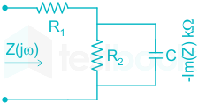
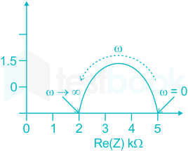
For the circuit shown, the locus of the impedance Z(jω) is plotted as ω increases from zero to infinity. The values of R1 and R2 are:


  1. ((a))

    R1 = 2 kΩ, R2 = 3 kΩ

  2. ((b))

    R1 = 5 kΩ, R2 = 2 kΩ

  3. ((c))

    R1 = 5 kΩ, R2 = 2.5 kΩ

  4. ((d))

    R1 = 2 kΩ, R2 = 5 kΩ

Show Answer
Answer: ((a))

R1 = 2 kΩ, R2 = 3 kΩ

Correct answer is option (1): R1 = 2K , R2 = 3k

Solution:

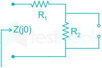
At ω= 0 rad/sec

  • Capacitor will be open circuited ; XC=1ωC=X_{C}= \frac{1}{ω C}= ∞

Impedance, Z(j0)=R1+R2Z(j0)= R_{1}+ R_{2}

From the graph ; 

Z(j0)=5KΩ R1+R2=5KΩZ(j0)= 5K Ω\ R_{1}+R_{2}=5K Ω                                   

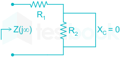
At ω= ∞ rad/sec:

Capacitor will be short circuited : Xc=1ωC=0X_{c}= \frac{1}{\omega C}= 0 

Impedance, 

Z(j)=R1=2KΩ  R1+R2=5KΩ R2=3KΩZ(j\infty)= R_{1}= 2 KΩ\ \ R_{1}+R{2}= 5 KΩ\ \rightarrow R_{2}= 3KΩ

Hence, R1 = 2 K Ω and R2 = 3 K Ω

46

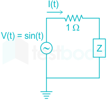
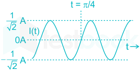
Consider the circuit shown in the figure with input V(t) in volts. The sinusoidal steady state current I(t) flowing through the circuit is shown graphically (where 𝑡 is in seconds). The circuit element Z can be ________.


  1. ((a))

    a capacitor of 1 F

  2. ((b))

    an inductor of 1 H

  3. ((c))

    a capacitor of √3 F

  4. ((d))

    an inductor of √3 H

Show Answer
Answer: ((b))

an inductor of 1 H

Correct answer is option (2): an inductor of 1H.

Explanation:

As per the given graph, the current through the element I(t) is lagging, it implies that the element is inductor.

I(t)=V(t)Zo  I(t)=sin(t)ZoI(t)= \frac{V(t)}{Z_{o}}\ \ I(t)= \frac{sin(t)}{Z_{o}}          

The maximum value of the current   I(t)max=12I(t)_{max} = \frac{1}{\sqrt{2}}

Zo=V(t)I(t) =112 =2|Z_{o}|=\frac{|V(t)|}{|I(t)|}\ =\frac{1}{\frac{1}{\sqrt{2}}}\ =\sqrt{2}

As per the circuit given,

Zo = R + jωL

Zo=R2+(jωL)2|Z_{o}|=\sqrt{R^{2}+(j ω L)^{2}}

2=1+ω2L2\sqrt{2}=\sqrt{1+ ω^{2}L^{2}}

Given, ω = 1 rad/sec

2=1+L2 \sqrt{2} = \sqrt{1+L^{2}}

2 = 1 + L2

L = 1 H

47

Consider an ideal long channel nMOSFET (enhancement-mode) with gate length 10 µm and width 100 µm. The product of electron mobility (µn) and oxide capacitance per unit area (COX) is µn COX = 1 mA/V2 . The threshold voltage of the transistor is 1 V. For a gate-to-source voltage VGS = [2 − sin (2t)] V and drain-to-source voltage VDS = 1 V (substrate connected to the source), the maximum value of the drain-to-source current is ________.

  1. ((a))

    40 mA

  2. ((b))

    20 mA

  3. ((c))

    15 mA

  4. ((d))

    5 mA

Show Answer
Answer: ((c))

15 mA

Correct answer is option (c)

**Concept:**​

Mode of operations of nMOSFET

  • If, VDS > (VGS - VT)   nMOSFET is operating in Saturation mode.
  • If, VDS < (VGS - VT)   nMOSFET is operating in Linear mode.
  • Here, ​ VDS  is Drain to source voltage , VGS  is Gate to Source voltage and VT is the required Threshold voltage.

​Expressions of Drain to Source current in different mode of operation.

​Linear mode:

 ID=μnCoxWL(VGSVT)VDS12VDS2I_{D} =μ_{n}C_{ox}\frac{W}{L}{(V_{GS}-V_{T})V_{DS}-\frac{1}{2}V_{DS}^{2}}

Saturation mode:

 ID=μnCoxW2L(VGSVT)2I_{D} =μ_{n}C_{ox}\frac{W}{2L}(V_{GS}-V_{T})^{2}


Calculation:

Given,

L= 10 μm ,

W= 100 μm , 

μnCox= 1 mA/V2,

VT= 1V,

VDS = 1V

VGS= [2 - sin(2t)]

VGS(max) = 3 v

VGS(min)= 1 V

here, VDS > (VGS - VT) condition will not be satisfied

Hence, nMOSFET is in Linear region

IDmax=μnCoxWL(VGSVT)VDS12VDS2I_{D_{max}} =\mu_{n}C_{ox}\frac{W}{L}{(V_{GS}-V_{T})V_{DS}-\frac{1}{2}V_{DS}^{2}}

=1mA/V2×10[(31)112×1)]=1 mA/V^{2}\times 10[(3-1)1- \frac{1}{2}\times1)]

= 10[1.5] mA = 15 mA

Hence, the maximum value of the drain-to-source current is 15 mA

48

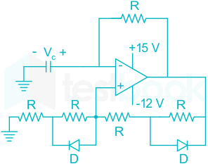
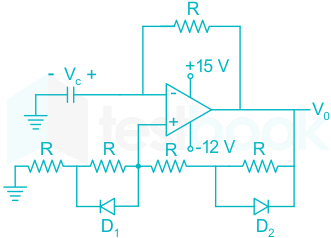
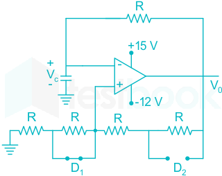
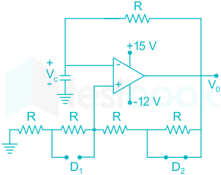
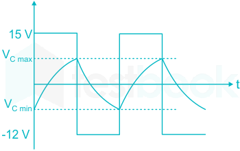
For the following circuit with an ideal OPAMP, the difference between the maximum and the minimum values of the capacitor voltage (Vc) is __________.

  1. ((a))

    15 V

  2. ((b))

    27 V

  3. ((c))

    13 V

  4. ((d))

    14 V

Show Answer
Answer: ((c))

13 V

Correct answer is option (3)

Solution:

If, VO = 15V

D1 is ON

D2 is OFF

VUT=15×RR+2R=5VV_{UT}= \frac{15 \times R}{R + 2R}=5V

Capacitor will charge up to VUT 

VCmax=VUT=5VV_{Cmax}= V_{UT}= 5 V

If, VO = -12V

D1 is OFF

D2 is ON

VUT=12×2RR+2R=8VV_{UT}= \frac{-12 \times 2R}{R + 2R}=-8V

Capacitor will discharge up to VL

VCmin=VLT=8VV_{Cmin}= V_{LT}= -8V

 Difference between the maximum and the minimum values of the capacitor voltage (Vc):


VCmaxVCmin=5(8)=13VV_{Cmax}-V_{Cmin}= 5-(-8)=13V


Hence, answer to the question is 13 V.

49

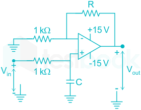
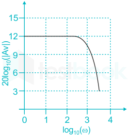
A circuit with an ideal OPAMP is shown. The Bode plot for the magnitude (in dB) of the gain transfer function (AV(jω) = Vout (jω)/Vin (jω)) of the circuit is also provided (here, ω is the angular frequency in rad/s). The values of R and C are ____________.


  1. ((a))

    R = 3 kΩ, C = 1 μF

  2. ((b))

    R = 1 kΩ, C = 3 μF

  3. ((c))

    R = 4 kΩ, C = 1 μF

  4. ((d))

    R = 3 kΩ, C = 2 μF

Show Answer
Answer: ((a))

R = 3 kΩ, C = 1 μF

Solution:

Correct answer is option(1)

At ω=0

Gain of the amplifier is maximum,

20log10(|AVmax|) = 12 dB

|AVmax| = 3.98

|AVmax| ≈ 4                                 .

Capacitor will be open circuited

Gain=(1+R1k) (1+R1k)=4 R=3K  Gain=(1+\frac{R}{1k})\ (1+\frac{R}{1k})=4\ R=3K \                                                    

As per the Bode plot corner frequency will be at,

log10c) = 3

ωc = 1000 rad/sec

ωc = 1/R3C

C = 1/(R3 × ωc

= 1/106

= 1 μF                                                

Hence, R = 3K and C= 1 μF.

50

For the circuit shown, the clock frequency is f0 and the duty cycle is 25%. For the signal at the Q output of the Flip-Flop, _______.

  1. ((a))

    frequency is f0/4 and duty cycle is 50%

  2. ((b))

    frequency is f0/4 and duty cycle is 25%

  3. ((c))

    frequency is f0/2 and duty cycle is 50%

  4. ((d))

    frequency is f0 and duty cycle is 25%

Show Answer
Answer: ((a))

frequency is f0/4 and duty cycle is 50%

The correct answer is option 1.

Concept:

2-bit Counter:

The 2-bit Counter With two T flip-flops in a chain you build a 2-bit counter. The output of the first flip-flop is connected to the input of the second flip-flop.

Explanation:

The given 2 bit counter,

The 2-bit count 

MSBLSB(J, K)
00
01
10
11

LSB 0, 1, 0, 1

For JK flip-flop (FF), 00 will not change the state.

So, output frequency = f0/2  

Two-time change of state and duty cycle = 50%.

The output frequency is:

The output frequency is= (f0/2 )/2

The output frequency is= f0/4.

Hence the correct answer is frequency is f0/4 and duty cycle is 50%.

51

Consider the following series:

Σn=1ndcn\Sigma_{n=1}^{\infty}\frac{n^d}{c^n}

For which of the following combinations of c, d values does this series converge?

  1. ((a))

    c = 1, d  = -1

  2. ((b))

    c = 2, d = 1

  3. ((c))

    c = 0.5, d = -10

  4. ((d))

    c = 1, d = -2

Show Answer
Answer: ((a))

c = 1, d  = -1

It is a MSQ question.

Correct answers would be option(2) and option (4)

Concept:

To check whether the given expression converges or not we will apply Ration test and P test.

Ratio Test:

Let an is the given expression.

Let L=limnan+1anL=\lim_{n \mapsto \infty }|\frac{a_{n+1}}{a_{n}}|

if L<1, then the series Converges

if L>1, then the series Diverges

if L<1, then the test is Inconclusive.

P series test:

 n=11np=11p+12p+13p+.....\sum_{n=1}^{\infty }\frac{1}{n^{p}}= \frac{1}{1^{p}}+\frac{1}{2^{p}}+\frac{1}{3^{p}}+.....  where p> 0 by definition

If p > 1 , then the series converges. If 0 < p <= 1 , then the series diverges.

Calculation:

Option (1): Substitute c= 1, d= -1

Perform  test:

n=1ndcn =n=1n11n =n=11n\sum_{n=1}^{\infty }\frac{n^{d}}{c^{n}}\ =\sum_{n=1}^{\infty }\frac{n^{-1}}{1^{n}}\ =\sum_{n=1}^{\infty }\frac{1}{n}   

As, p=1 , hence series will diverge.

Hence, option (1) is incorrect.

Option (2):

Substitute c=2, d= 1.

Perform Ration test

limnan+1an=limnn+12n+1×2nn=12 \lim_{n \mapsto \infty }|\frac{a_{n+1}}{a_{n}}|=\lim_{n \mapsto \infty}\frac{n+1}{2^{n+1}}\times \frac{2^{n}}{n}=\frac{1}{2}

​​​​As, L < 1 , the series converges.

Hence, option (2) is correct 

Option (3): 

​Substitute c= 0.5, d= -10

Perform Ratio test;

an=n10(0.5)n limnan+1an=limn(n+1)10(0.5)n+1×0.5nn10=10.5=2 \sum a_{n}= \sum \frac{n^{-10}}{(0.5)^{n}}\ \lim_{n \mapsto \infty }|\frac{a_{n+1}}{a_{n}}|=\lim_{n \mapsto \infty}\frac{(n+1)^{-10}}{(0.5)^{n+1}}\times \frac{0.5^{n}}{n^{10}}=\frac{1}{0.5}=2

As L>1, the series will diverge.

Hence, option (3) is incorrect.

Option (4):

​Substitute c= 1, d= -2

Perform P test:

  • an=n2(1)n=1n2\sum a_{n}= \sum \frac{n^{-2}}{(1)^{n}}=\sum\frac{1}{n^{2}}
  • Here, p > 1 , therefore the series converges.
  • Hence, option (4) is correct.
52

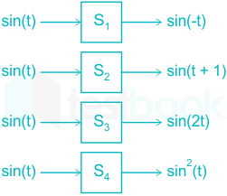
The outputs of four systems (S1, S2, S3, and S4) corresponding to the input signal sin(t), for all time t, are shown in the figure.

Based on the given information, which of the four systems is/are definitely NOT LTI (linear and time-invariant)?

  1. ((a))

    S1

  2. ((b))

    S2

  3. ((c))

    S3

  4. ((d))

    S4

Show Answer
Answer: ((a))

S1

Concept:

For an LTI system, the following results hold true:

  • The same form of the sinusoidal signal is produced at the output.
  • The only change will be in magnitude and phase.
  • ∴ If a system produces frequencies in the output other than those which are in input, then that system can’t be called as the ‘Linear shift-invariant’ system.


Analysis:

sintS1sin(t)=sint\sin t \rightarrow \boxed{S_1} \rightarrow \sin (-t) = - \sin t

sintS2sin(t+1)\sin t \rightarrow \boxed{S_2} \rightarrow \sin (t + 1)

sintS3sin(2t)\sin t \rightarrow \boxed{S_3} \rightarrow \sin (2t )

sintS4sin2(t)=1cos2t2\sin t \rightarrow \boxed{S_4} \rightarrow \sin^2 (t ) = \frac{1 - \cos 2t}{2}

Since, LTI system does not change the frequency of sinusoidal input,

So S3 and S4 are definitely not LTI as input and output sinusoidal frequencies are different.

53

Select the CORRECT statement(s) regarding semiconductor devices.

  1. ((a))

    Electrons and holes are of equal density in an intrinsic semiconductor at equilibrium.

  2. ((b))

    Collector region is generally more heavily doped than Base region in a BJT.

  3. ((c))

    Total current is spatially constant in a two terminal electronic device in dark under steady state condition.

  4. ((d))

    Mobility of electrons always increases with temperature in Silicon beyond 300 K.

Show Answer
Answer: ((a))

Electrons and holes are of equal density in an intrinsic semiconductor at equilibrium.

Remark: It is a MSQ question.

Correct answers are option (1) and option (3)

Explanation:

Option(1):

  • An intrinsic semiconductor is an undoped semiconductor.
  • For an intrinsic semiconductor, the concentration of electrons in the conduction band is equal to the concentration of holes in the valence band at thermal equilibrium.
  • Hence, option (1) is correct.

Option(2):

  • ​Collector region is generally lightly doped than base region in BJT
  • Hence, option (2) is incorrect.

Option(3):

  • The total current due to injected minority carrier ( diffusion current ) and majority carrier ( drift current ) is spatially constant in two terminal electronic device, however they individually will be spatially different under dark and steady state condition.

  • Hence, Option(3) is correct.
  • ​Option(4):

​Mobility of electrons always decreases with temperature in Silicon beyond 300 K.

Hence, option(4) is incorrect​

54

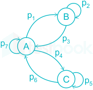
A state transition diagram with states A, B, and C, and transition probabilities p1, p2, … , p7 is shown in the figure (e.g., p1 denotes the probability of transition from state A to B). For this state diagram, select the statement(s) which is/are universally true.

  1. ((a))

    p+ p3 = p5 + p6

  2. ((b))

    p1 + p3 = p4 + p6

  3. ((c))

    p1 + p4 + p7 = 1

  4. ((d))

    p2 + p5 + p7​ = 1

Show Answer
Answer: ((a))

p+ p3 = p5 + p6

The correct answer is option 1 and option 3.

Concept:

The given data, 

A state transition diagram with states A, B, and C, and transition probabilities p1, p2, …, p7

From state A outgoing transitions are,

P7 A, P1 B, P4 C are equal to 1.

P1 + P4 + P7 =1

From state B outgoing transitions are,

P2 A, P3 B are equal to 1.

P2+P3=1

From state C outgoing transitions are,

P6A, P5C are equal to 1.

P5+P6=1

Option 1: p2 + p3 = p5 + p6

True, P2+P3=P5+P6

From State B and State, C are the same number of transitions and those are similar.

Option 2: p1 + p3 = p4 + p6

False, P1+P3=P4+P6

We can not equalize those probabilities and are not similar or not equal.

Option 3: p1 + p4 + p7 = 1

True, p1 + p4 + p7 = 1 

From state A we can find the sum of all probabilities is equal to 1.

Option 4: p2 + p5 + p7​ = 1

False, p2 + p5 + p7​ = 1

We can not equalize those probabilities and are not similar or not equal.

Hence the correct answer is option 1 and option 3.

55

Consider a Boolean gate (D) where the output Y is related to the inputs A and B as, Y = A + B̅, where + denotes logical OR operation. The Boolean inputs ‘0’ and ‘1’ are also available separately. Using instances of only D gates and inputs ‘0’ and ‘1’, __________ (select the correct option(s)).

  1. ((a))

    NAND logic can be implemented

  2. ((b))

    OR logic cannot be implemented

  3. ((c))

    NOR logic can be implemented

  4. ((d))

    AND logic cannot be implemented

Show Answer
Answer: ((a))

NAND logic can be implemented

The correct answer is option 1 and option 3.

Concept:

The given function is,

y=A+B' = (A'B)'

f(A,B)= A+B'

As 0 and 1 are available.

f(0,B)= A+B'= B'= NOT Gate.

f(A,B')= A+(B')' = A+B= OR Gate.

f(o,f(A,B'))=0 +(A+B)'= NOR Gate.

f(A',B)=A'+B'= (A.B)' =NAND Gate.

f(0,f(A',B)) = 0+((A.B)')'= A.B= AND Gate.

With the combination of OR and NOT, NOR gate can be implemented. Since NOR gate is universal logic gate, so all the functions can be implemented. 

Hence, we can implement NOT Gate we can also implement OR, AND, NOR and NAND Gate.

Hence the correct answer is option 1 and option 3.

56

Two linear time-invariant systems with transfer functions

G1(s)=10s2+s+1\rm G_1(s)=\frac{10}{s^2+s+1} and G2(s)=10s2+s10+10\rm G_2(s)=\frac{10}{s^2+s\sqrt{10}+10}

have unit step responses y1(t) and y2(t), respectively. Which of the following statements is/are true?

  1. ((a))

    y1(t) and y2(t) have the same percentage peak overshoot.

  2. ((b))

    y1(t) and y2(t) have the same steady-state value.

  3. ((c))

    y1(t) and y2(t) have the same damped frequency of oscillation.

  4. ((d))

    y1(t) and y2(t) have the same 2% settling time.

Show Answer
Answer: ((a))

y1(t) and y2(t) have the same percentage peak overshoot.

Calculation:

Given 

G1(s)=10s2+s+1  \rm G_1(s)=\frac{10}{s^2+s+1} \ \   &  G2(s)=10s2+s10+10  \rm G_2(s)=\frac{10}{s^2+s√{10}+10} \ \

Comparing standard second-order equation 

S2 + 2 ζ wn S + Wn2 = 0

Wn1 = 1,  2 ζ1 Wn1  = 1

ζ1 = 0.5

Wn2 = √ 10

2 ζ2 Wn2 = √ 10

ζ2 = 0.5

Percentage peak overshoot:

% Mp = eπζ1ζ2  \dfrac {e^{-\pi ζ }}{\sqrt {1-ζ ^2}}\ \

Percentage peak overshoot is depend only on ζ 

ζ1 = ζ2 

Therefore % Mp is the same as for both y1(t) and y2(t)         (option 1 is correct)

Steady-state value: 

  lims0  sY(s)  lim _{s→ 0}~~sY(s)\ \

<br>

Y1(s)=10s(s2+s+1)  \rm Y_1(s)=\frac{10}{s(s^2+s+1)} \ \  and  Y2(s)=10s(s2+s10+10)  \rm Y_2(s)=\frac{10}{s(s^2+s√{10}+10)} \ \

Steady-state value of y1(t) →  10

Steady-state value of y1(t) →  1 

Therefore the steady-state values of both systems are different          (option 2 is incorrect)


Damped frequency of oscillation (Wd): 

  Wd=Wn(1ζ2    W_d=W_n\sqrt {(1-ζ ^2}\ \ \ \

Wd1=Wn11ζ12    W_{d1}=W_{n1} \sqrt {1-ζ_1 ^2}\ \ \ \

Wd1=1114  =32=0.86    W_{d1}=1 \sqrt {1-\dfrac {1}{4}}\ \ =\dfrac {\sqrt 3}{2}= 0.86\ \ \ \

Wd2=10114  =10×32=2.73    W_{d2}=\sqrt{10} \sqrt {1-\dfrac {1}{4}}\ \ =\sqrt {10} \times \dfrac {\sqrt 3}{2}= 2.73\ \ \ \

Wd1 ≠ Wd2        (option 2 is incorrect)

Settling time (ts):

For 2% tolerance band 

ts=4ζWn  t_s=\dfrac{4}{ζ W_n}\ \

By putting values of ζ and Wn

ts1=412×1=8  sec    t_{s1}= \dfrac {4}{\dfrac {1}{2}\times 1}=8 \ \ sec\ \ \ \

ts2=412×10=2.53  sec   t_{s2}= \dfrac {4}{\dfrac {1}{2}\times \sqrt {10}}=2.53\ \ sec\ \ \space

ts1 ≠ ts2     (option 4 is incorrect)

57

A waveguide consists of two infinite parallel plates (perfect conductors) at a separation of 10-4 cm, with air as the dielectric. Assume the speed of light in air to be 3 × 10⁸ m/s. The frequency/frequencies of TM waves which can propagate in this waveguide is/are _______.

  1. ((a))

    6 × 1015 Hz

  2. ((b))

    0.5 × 1012 Hz

  3. ((c))

    8 × 1014 Hz

  4. ((d))

    1 × 1013 Hz

Show Answer
Answer: ((a))

6 × 1015 Hz

Concept:

Cut off frequency: Every waveguide has a cut off frequency below which there is no propagation.

For parallel plate cut off frequency is given as:

fc=mc2a  Hz  f_c= \dfrac {m c}{2 a} \ \ Hz \space \space

Calculation:

The mode that propagates at the lowest cut off frequency is TM1 mode

fc  TM1=c2a=3×1082×104=1.5×10¹⁴  Hz f_{{c}\ \ _{TM_1}}=\dfrac {c}{2a}=\dfrac {3× {10}^8}{2× {10}^{-4}}=1.5× {10}^{14}\ \ Hz \space

For propagation,

f > fc 

Therefore the frequency is greater than 1.5 × 1014 Hz can propagate in the waveguide

In the given option 6× 10¹⁵ Hz and 8 × 1014 Hz can propagate in waveguide.

58

The value of the integral

D3(x2+y2) dxdy  \rm \iint_D 3(x^2+y^2)\ dxdy \ \

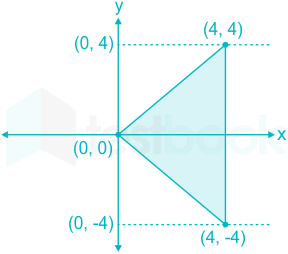
where D is the shaded triangular region shown in the diagram, is _____ (rounded off to the nearest integer).

59

A linear 2-port network is shown in Fig. (a). An ideal DC voltage source of 10 V is connected across Port 1. A variable resistance R is connected across Port 2. As R is varied, the measured voltage and current at Port 2 is shown in Fig. (b) as a V2 versus -I2 plot. Note that for V2 = 5 V, I2 = 0 mA, and for V2 = 4 V, I= −4 mA.

When the variable resistance R at Port 2 is replaced by the load shown in Fig. (c), the current I2 is _______ mA (rounded off to one decimal place).


60

For a vector x̅ = [x[0], x[1],......x[7]] the 8-point discrete Fourier transform (DFT) is denoted by X̅ = DFT (x̅) = X[0], X[1], ...., X[7]], where

X[k]=n=07x[n] exp(j2π8nk) \rm X[k]=\sum_{n=0}^{7}x[n]\ exp\left(-j\frac{2\pi}{8}nk\right) \space

Here j = √-1, if X̅ = [1, 0, 0, 0, 2, 0, 0, 0] and y̅ = (DFT (x̅)), then the value of y[0] is ________ (rounded off to one decimal place).

61

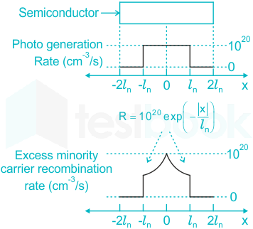
A p-type semiconductor with zero electric field is under illumination (low level injection) in steady state condition. Excess minority carrier density is zero at x = ±,2 ln where ln = 10-4 cm is the diffusion length of electrons. Assume electronic charge, q = −1.6 × 10⁻¹⁹ C. The profiles of photo-generation rate of carriers and the recombination rate of excess minority carriers (R) are shown. Under these conditions, the magnitude of the current density due to the photo-generated electrons at x = +2 ln is _________ mA/cm2 (rounded off to two decimal places).

62

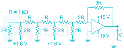
Consider the circuit shown with an ideal OPAMP. The output voltage Vo is __________V (rounded off to two decimal places).

63

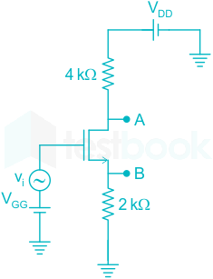
Consider the circuit shown with an ideal long channel nMOSFET (enhancement-mode, the substrate is connected to the source). The transistor is appropriately biased in the saturation region with VGG and VDD such that it acts as a linear amplifier. vi is the small-signal ac input voltage. vA and vB represent the small-signal voltages at nodes A and B, respectively. The value of vAvB \dfrac{v_A}{v_B} \space ,is ________ (rounded off to one decimal place).

64

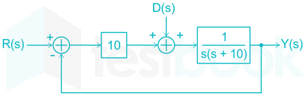
The block diagram of a closed-loop control system is shown in the figure. R(s), Y(s), and D(s) are the Laplace transforms of the time-domain signals r(t), y(t), and d(t), respectively. Let the error signal be defined as e(t) = r(t) − y(t). Assuming the reference input r(t) = 0 for all t, the steady-state error e(∞), due to a unit step disturbance d(t), is _________ (rounded off to two decimal places).

65

Consider a channel over which either symbol xA or symbol xB is transmitted. Let the output of channel Y be the input to a maximum likelihood (ML) detector at the receiver. The conditional probability density functions for 𝑌 given xA and xB are:

fYxA(y)=e(y+1)u(y+1)\rm f_{Y|x_A}(y)=e^{-(y+1)}u(y+1)

fYxB(y)=e(y1)(1u(y1))\rm f_{Y|x_B}(y)=e^{(y-1)}(1-u(y-1))

where u(⋅) is the standard unit step function. The probability of symbol error for this system is _________ (rounded off to two decimal places).

Attempt this paper under real exam conditions

Timed interface, section switching, instant scoring, and question-by-question analytics — free.

Start Timed Attempt