Official Paper

GATE EC 2020 Official Paper (Previous Year Paper)

65 questions · 180 minutes · with answers · free

General Aptitude (10 questions)

1

The untimely loss of life is a cause of serious global concern as thousands of people get killed ______ accidents every year while many other die ________ diseases like cardiovascular disease, cancer, etc

  1. ((a))

    in, of

  2. ((b))

    from, of

  3. ((c))

    during, from

  4. ((d))

    from, from

Show Answer
Answer: ((a))

in, of

The correct answer is Option 1) i.e. in, of

Let's take the second blank first, we have two choices die of/from, traditionally, 'die of' refers to dying as the result of a disease, and 'die from' refers to death as a result of an external cause such as an accident or a disaster.

For example:

  • My uncle died of cancer.
  • She died of old age.
  • He died from starvation.

Therefore, 'of' is the best fit for the second blank and as a result, we can easily negate option 3 and 4. Now we are left with two choices for the first blank. 'In' here is the most appropriate as per the context of the sentence, 'from' is used to indicate the source or provenance of someone or something and 'accident' is neither a source or a medium it is an unfortunate event.

Complete Sentence: The untimely loss of life is a cause of serious global concern as thousands of people get killed in accidents every year while many other die of diseases like cardiovascular disease, cancer, etc
2

​He was not only accused of theft_______of conspiracy.

  1. ((a))

    rather

  2. ((b))

    but also

  3. ((c))

    but even

  4. ((d))

    rather than

Show Answer
Answer: ((b))

but also

The correct answer is Option 2) i.e. but also

"Not only.....But also" is correlative conjunction which are used in a pair. Correlative conjunctions are pairs such as neither . . . nor, not . . . only, and but . . . also. These conjunctions connect two balanced clauses, phrases, or words. The two elements that correlative conjunctions connect are usually similar in length and grammatical structure.

This Conjunction pair (not only....but also) is used to present two related pieces of information. Both pieces of information are being presented by the writer as surprising or unexpected, with the second one being even more surprising than the first. The first piece of information(accused of theft) will be followed by the second one (conspiracy).

Complete Sentence: He was not only accused of theft but also of conspiracy.

3

Select the word that fits the analogy:

Explicit : Implicit :: Express :

  1. ((a))

    Impress

  2. ((b))

    Repress

  3. ((c))

    Compress

  4. ((d))

    Suppress

Show Answer
Answer: ((b))

Repress

The correct answer is option 2) i.e. Repress.

From the first part of the analogy, it becomes clear that the two words are opposite in meaning i.e. 'Explicit' is the antonym of 'Implicit'. Similarly, the antonym of 'Express' will be ''Repress'.

The meaning of the words are given below:

  • Explicit: fully revealed or expressed without vagueness, implication, or ambiguity : leaving no question as to meaning or intent.
  • Implicit: involved in the nature or essence of something though not revealed, expressed, or developed.
  • Express: to make known the opinions or feelings of (oneself).
  • Repress:  to prevent the natural or normal expression(feelings), activity, or development of.
4

The Canadian constitution requires that equal importance be given to English and French. Last year, Air Canada lost a lawsuit and had to pay a six-figure fine to a French-speaking couple after they filed complaints about formal in-flight announcements in English lasting 15 seconds, as opposed to informal 5-second messages in French.

The French-speaking couple were upset at

  1. ((a))

    the in-flight announcements being made in English. 

  2. ((b))

    the English announcements being clearer than the French ones. 

  3. ((c))

    the English announcements being longer than the French ones.

  4. ((d))

    equal importance being given to English and French

Show Answer
Answer: ((c))

the English announcements being longer than the French ones.

The correct answer is option 3) i.e. the English announcements being longer than the French ones.

After reading the passage we can easily comprehend that the french-speaking couple filed a lawsuit against Air Canada because they were upset at the English announcements being longer than the French ones. It has been mentioned clearly in the passage "formal in-flight announcements in English lasting 15 seconds, as opposed to informal 5-second messages in French.".

5

A superadditive function f(⋅) satisfies the following property:

f(x1+x2)f(x1)+f(x2)f\left( {{x_1} + {x_2}} \right) \ge f\left( {{x_1}} \right) + f\left( {{x_2}} \right)

Which of the following functions is a superadditive function for x > 1?

  1. ((a))

    ex

  2. ((b))

    √x

  3. ((c))

    1/x

  4. ((d))

    e-x

Show Answer
Answer: ((a))

ex

Given that a super additive function satisfies the following property:

f(x1 + x2) ≥ f(x1) + f(x2)

Checking for each option, i.e.

Option 1:

Let us take x1 = 2, and x2 = 4

ex1+x2 = e 2+4 = e6 = 403.42

ex1+ex2=e2+e4=61.98{e^{{x_1}}} + {e^{{x_2}}} = {e^2} + {e^4} = 61.98 

Since ex1+x2>ex1+ex2{e^{{x_1} + {x_2}}} > {e^{{x_1}}} + {e^{{x_2}}}

ex satisfies the superadditive property.

Option 2:

If x\sqrt x  is to be a super-additive function, then it must also satisfy:

x1+x2x1+x2\sqrt {{x_1} + {x_2}} \ge \sqrt {{x_1}} + \sqrt {{x_2}}

Again for x1 = 2 and x2 = 4, we get:

2+4=6=2.44\sqrt {2 + 4} = \sqrt 6 = 2.44

2+4=1.414+2=3.414\sqrt 2 + \sqrt 4 = 1.414 + 2 = 3.414

x1+x2<x1+x2\sqrt {{x_1} + {x_2}} < \sqrt {{x_1}} + \sqrt {{x_2}}

∴ √x does not follow the super-additive property.

Option 3: 1/x

For x1 = 2 and x2 = 4

1x1+x2=16=0.166\frac{1}{{{x_1} + {x_2}}} = \frac{1}{6} = 0.166

1x1+1x2=12+14=34=0.75\frac{1}{{{x_1}}} + \frac{1}{{{x_2}}} = \frac{1}{2} + \frac{1}{4} = \frac{3}{4} = 0.75

Since, 1x1+x2<1x1+1x2\frac{1}{{{x_1} + {x_2}}} < \frac{1}{{{x_1}}} + \frac{1}{{{x_2}}}

1/x does not satisfy the superadditive property.

Option 4:

Checking for e-x

For x1 = 2, x2 = 4

e(x1+x2)=e6=0.0024{e^{ - \left( {{x_1} + {x_2}} \right)}} = {e^{ - 6}} = 0.0024

ex1=0.135{e^{ - {x_1}}} = 0.135

ex2=0.028{e^{ - {x_2}}} = 0.028

Since, e(x1+x2)<ex1+ex2{e^{ - \left( {{x_1} + {x_2}} \right)}} < {e^{ - {x_1}}} + {e^{ - {x_2}}}

e-x does not satisfy the superadditive property.

6

The global financial crisis in 2008 is considered to be the most serious worldwide financial crisis, which started with the sub-prime lending crisis in USA in 2007. The sub-prime lending crisis led to the banking crisis in 2008 with the collapse of Lehman Brothers in 2008. The sub-prime lending refers to the provision of loans to those borrowers who may have difficulties in repaying loans, and it arises because of excess liquidity following the East Asian crisis.

Which one of the following sequences shows the correct precedence as per the given passage?

  1. ((a))

    East Asian crisis →  subprime lending crisis → banking crisis → global financial crisis. 

  2. ((b))

    Subprime lending crisis → global financial crisis → banking crisis → East Asian crisis. 

  3. ((c))

    Banking crisis → subprime lending crisis → global financial crisis → East Asian crisis. 

  4. ((d))

    Global financial crisis → East Asian crisis → banking crisis → subprime lending crisis.

Show Answer
Answer: ((a))

East Asian crisis →  subprime lending crisis → banking crisis → global financial crisis. 

The correct answer is option 1) i.e.East Asian crisis →  subprime lending crisis → banking crisis → global financial crisis.

After reading the passage and going through the options (cursory look), we can easily comprehend that we need to select the precedence order on the basis of time( the event that happened first will be on the leftmost side). Let's see the following lines given in the passage "The global financial crisis in 2008 is considered to be the most serious worldwide financial crisis,", so it is clear that 'global financial crisis' is the final result that occurred because of some series of event that took place in the past. Let's connect these chain of events- Excess liquidity resulted in East Asian crises and to compensate this crisis 'sub-prime lending' came into play (provision of loans to those borrowers who may have difficulties in repaying loans), the sub-prime lending crisis led to the banking crisis in 2008 with the collapse of Lehman Brothers in 2008, finally all this resulted in the global financial crisis.

7

It is quarter past three in your watch. The angle between the hour hand and the minute hand is

  1. ((a))

    0° 

  2. ((b))

    7.5° 

  3. ((c))

    15° 

  4. ((d))

    22.5° 

Show Answer
Answer: ((b))

7.5° 

Concept:

The angle between the hour and the minute hand is given by the formula:

θ=11m230hθ=|\frac{11m}{2}-30h|

h = Hours (≤ 12)

m = minutes (≤ 60)

Calculation:

The time quarter past 3 is 3:15, i.e.

h = 3

m = 15

The angle between the hour and minute hand will be:

θ=11×15230×3θ=|\frac{11\times15}{2}-30\times3|

θ = 7.5°

8

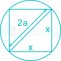
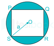
A circle with center O is shown in the figure. A rectangle PQRS of the maximum possible area is inscribed in the circle. If the radius of the circle is a, then the area of the shaded portion is _______.

  1. ((a))

    πa2 – a2

  2. ((b))

    πa2 - √2a2

  3. ((c))

    πa2 – 2a2

  4. ((d))

    πa2 – 3a2

Show Answer
Answer: ((c))

πa2 – 2a2

Concept:

Area of a circle is given by:

A = πr2

r = radius

Area of a rectangle is given by:

A = a × b

a = length of the rectangle

b = breadth of the rectangle

For the rectangle to have a maximum area, the two sides must be of equal length, i.e.

For a = b, the area will be maximum.

Application:

The area of the rectangle will be maximum when both the sides are of equal length, as shown:

Applying Pythagoras theorem, we can write:

x2 + x2 = (2a)2

2x2 = 4a2

x=2ax = \sqrt 2 a

The maximum area of the rectangle wll be:

A = x2 = 2a2

Area of circle = πa2

The area of the shaded portion will be the difference between the two, i.e.

Area of the circle – Area of rectangle

= πa2 – 2a2

9

a, b, c are real numbers. The quadratic equation ax2 – bx + c = 0 has equal roots, which is β, then
  1. ((a))

    β = b/a

  2. ((b))

    β2 = ac

  3. ((c))

    β3 = bc/(2a2)

  4. ((d))

    b2 ≠ 4ac

Show Answer
Answer: ((c))

β3 = bc/(2a2)

Concept:

For a quadratic equation of the form:

ax2 – bx + c = 0, the roots will be given by:

x=b±b24ac2ax = \frac{{b \pm \sqrt {{b^2} - 4ac} }}{{2a}} 

For the roots to be equal, b2 – 4ac should equal 0, i.e.

b2 = 4ac     ---(1)

Given that the value of the equal root is β, i.e.

β=b2a\beta = \frac{b}{{2a}}         ---(2)

From the above condition, we conclude that option (1) is not correct.

Squaring equation (2), we get:

β2=b2(2a)2{\beta ^2} = \frac{{{b^2}}}{{{{\left( {2a} \right)}^2}}} 

Putting b2 from equation (1) in the above, we get:

β2=4ac(2a)2=4ac4a2{\beta ^2} = \frac{{4ac}}{{{{\left( {2a} \right)}^2}}} = \frac{{4ac}}{{4{a^2}}}

β2=ca{\beta ^2} = \frac{c}{a}

∴ option (2) is also incorrect.

Cubing equation (2), we can also write:

β3=b3(2a)3{\beta ^3} = \frac{{{b^3}}}{{{{\left( {2a} \right)}^3}}} 

With b2 = 4ac

b3 = 4abc

β3=4abc(2a)3\therefore {\beta ^3} = \frac{{4abc}}{{{{\left( {2a} \right)}^3}}}

β3=bc2a2{\beta ^3} = \frac{{bc}}{{2{a^2}}}

∴ Option (3) is correct.

Option (4) cannot be correct, because for the root to be equal, b2 = 4ac must satisfy.

10

The following figure shows the data of students enrolled in 5 years (2014 to 2018) for two schools P and Q. During this period, the ratio of the average number of the students enrolled in school P to the average of the difference of the number of students enrolled in schools P and Q is ______

  1. ((a))

    8 : 13

  2. ((b))

    23 : 8

  3. ((c))

    23 : 31

  4. ((d))

    31 : 23

Show Answer
Answer: ((b))

23 : 8

The average number of students enrolled in P will be:

Ap=3k;+;5k;+;5k;+;6k;+;4k5{A_p} = \frac{{3k; + ;5k ;+ ;5k ;+; 6k; + ;4k}}{5}

Ap = 4600

Similarly, The average number of students enrolled in Q will be:

AQ=4k;+;7k;+;8k;+;7k;+;5k5{A_Q} = \frac{{4k; +; 7k ;+; 8k ;+ ;7k; + ;5k}}{5}

AQ = 6200

Average of the difference in the number of students enrolled in P and Q will be:

[(4k - 3k) + (7k - 5k) + (8k - 5k) + (7k - 6k) + (5k - 4k)]/5 = 8k/5 = 1600

The required ratio will now be:

=ApAQAp= \frac{{{A_p}}}{{{A_Q} - {A_p}}}

=46001600=4616= \frac{{4600}}{{1600}} = \frac{{46}}{{16}}

= 23 : 8

Electronics and Communication Engineering (55 questions)

11

If v1, v2, …., v6 are six vectors in R4, which one of the following statements is FALSE?

  1. ((a))

    It is not necessary that these vectors span R4.

  2. ((b))

    These vectors are not linearly independent

  3. ((c))

    Any four of these vectors form a basis for R4

  4. ((d))

    If {v1, v3, v5, v6} span R4, then it forms a basis for R4.

Show Answer
Answer: ((c))

Any four of these vectors form a basis for R4

Concept:

Basis: it is defined as a subset of vectors within the space that are linearly independent i.e. it can’t be defined as a set of a linear combination of any other vectors.

Span: It is defined as the linear combination of linearly independent vectors within the space.

R4: It shows the space of 4 linearly independent vectors.

Analysis:

  1. R4 means that there are only 4 linearly independent vectors out of 6 vectors. So it is not necessary that these vectors span R4. (TRUE STATEMENT)

  2. All these vectors are not linearly independent because there are only 4 linearly independent vectors out of 6 vectors. (TRUE STATEMENT)

  3. Any four of these vectors can’t form a basis for R4 because only linearly independent vectors can form the basis for R4. Out of 6 vectors, only 4 vectors are linearly independent. So, this statement is wrong. (WRONG STATEMENT)

4) If {v1, v3, v5, v6} span R4, it means that vectors {v1, v3, v5, v6} are linearly independent, because span shows the linear combination of linearly independent vectors. Hence, it forms a basis for R4. (TRUE STATEMENT)

12

For a vector field A\vec A, which one of the following is FALSE?

  1. ((a))

    A\vec A is solenoidal if A=0\nabla \cdot \vec A = 0

  2. ((b))

    ×A\nabla \times \vec A is another vector field

  3. ((c))

    A\vec A is irrotational if 2A=0{\nabla ^2}\vec A = 0

  4. ((d))

    ×(×A)=(A)2A\nabla \times \left( {\nabla \times \vec A} \right) = \nabla \left( {\nabla \cdot \vec A} \right) - {\nabla ^2}\vec A

Show Answer
Answer: ((c))

A\vec A is irrotational if 2A=0{\nabla ^2}\vec A = 0

Explanation:

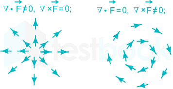
If a vector field A\vec A is solenoidal, it indicates that the divergence of the vector field is zero, i.e.

A=0\nabla \cdot \vec A = 0

If a vector field A\vec A is irrotational, it represents that the curl of the vector field is zero, i.e.

×A=0\nabla \times \vec A=0

If a field is scalar A then 2A=0{\nabla ^2}\vec A = 0 is a Laplacian function.

Important Vector identities:

×(×A)=(A)2A\nabla \times \left( {\nabla \times \vec A} \right) = \nabla \left( {\nabla \cdot \vec A} \right) - {\nabla ^2}\vec A

.(×A)=0\nabla .\left( {\nabla \times \vec A} \right) = 0 (Divergence of a vector field is always zero)

×(A)=0\nabla \times\left( {\nabla\vec A} \right) = 0 (Curl of a gradient is always zero)

13

The partial derivative of the function

f(x,;y,;z)=e1xcosy+xze1/(1+y2)f\left( {x,;y,;z} \right) = {e^{1 - x\cos y}} + xz{e^{ - 1/\left( {1 + {y^2}} \right)}}

With respect to x at the point (1, 0, e) is

  1. ((a))

    -1

  2. ((b))

    0

  3. ((c))

    1

  4. ((d))

    1e\frac{1}{e}

Show Answer
Answer: ((b))

0

Concept:

When the input of a function is made up of multiple variables, partial derivative is used to understand how the function changes as we let just one of the variable changes, keeping all the other variables as constant.

Application:

Given f(x,;y,;z)=e1xcosy+xze11+y2f\left( {x,;y,;z} \right) = {e^{1 - x\cos y}} + xz{e^{ - \frac{1}{{1 + {y^2}}}}}

Differentiating the above with respect to x and treating y and z as a constant, we get:

fx=e(1xcosy)ddx(1xcosy)+ze11+y2x(x)\frac{{\partial f}}{{\partial x}} = {e^{(1 - x\cos y)}} \cdot \frac{d}{{dx}}\left( {1 - x\cos y} \right) + z{e^{\frac{{ - 1}}{{1 + {y^2}}}}} \cdot \frac{\partial }{{\partial x}}\left( x \right)

fx=e(1xcosy)(cosy)+ze1y2+1\frac{{\partial f}}{{\partial x}} = {e^{\left( {1 - x\cos y} \right)}} \cdot \left( { - \cos y} \right) + z{e^{\frac{{ - 1}}{{{y^2} + 1}}}}

fx=cosye(1xcosy)+ze1y2+1\frac{{\partial f}}{{\partial x}} = - \cos y{e^{(1 - x\cos y)}} + z{e^{ - \frac{1}{{{y^2} + 1}}}}

At point (1, 0, e), the partial derivative gives a value:

\(\frac{{\partial f}}{{\partial x}}|_\left( {1,0,e} \right); = - \cos \left( 0 \right);{e^{(1 - \cos 0)}} + e.{e^{ - \frac{1}{1}}}\)

= -1e0 + e.e-1

= -1 + 1

\(\frac{{\partial f}}{{\partial x}}|_\left( {1,0,e} \right); =0\)

14

The general solution of d2ydx26dydx+9y=0\frac{{{d^2}y}}{{d{x^2}}} - 6\frac{{dy}}{{dx}} + 9y = 0 is

  1. ((a))

    y=C1e3x+C2e3xy = {C_1}{e^{3x}} + {C_2}{e^{ - 3x}}

  2. ((b))

    y=(C1+C2x)e3xy = \left( {{C_1} + {C_2}x} \right){e^{ - 3x}}

  3. ((c))

    y=(C1+C2x)e3xy = \left( {{C_1} + {C_2}x} \right){e^{3x}}

  4. ((d))

    y=C1e3xy = {C_1}{e^{3x}}

Show Answer
Answer: ((c))

y=(C1+C2x)e3xy = \left( {{C_1} + {C_2}x} \right){e^{3x}}

Concept:

For a second-order differential function, the characteristic equation will have two roots D1 and D2. The roots can have three possible forms i.e.

  • Real, distinct roots, D1 ≠ D2
  • Complex roots, D1, D2 = a ± ib
  • Double roots D1 = D2 = 0

The solution for the second-order differential equation with equal roots of the characteristic equation is given by:

y=(C1+C2x)eD1xy = \left( {{C_1} + {C_2}x} \right){e^{{D_1x}}}

Application:

Given: d2ydx26dydx+9y=0\frac{{{d^2}y}}{{d{x^2}}} - \frac{{6dy}}{{dx}} + 9y = 0

The characteristic equation will be:

D2 – 6D + 9 = 0

(D - 3)2 = 0

D = 3, 3

Since the roots are real and equal, the general solution of the given differential equation will be:

y=(C1+C2x)e3xy = \left( {{C_1} + {C_2}x} \right){e^{3x}}

Important Point:

If two roots are real and distinct (i.e. D1 ≠ D2), the general solution will be:

y=C1eD1t+C2eD2ty = {C_1}{e^{{D_1}t}} + {C_2}{e^{{D_2}t}}

If the roots of the characteristic equation are complex (i.e. D1, 2 = a ± ib), the general solution to the differential equation will be:

y=C1eatcos(bt)+C2eatsin(bt)y = {C_1}{e^{at}}\cos \left( {bt} \right) + {C_2}{e^{at}}\sin \left( {bt} \right)

15

The output y[n] of a discrete-time system for an input x[n] is

y[n]=maxknx[k]y\left[ n \right] = \mathop {\max }\limits_{ - \infty \le k \le n} \left| {x\left[ k \right]} \right|

The unit impulse response of the system is

  1. ((a))

    0 for all n

  2. ((b))

    1 for all n

  3. ((c))

    unit step signal u[n]

  4. ((d))

    unit impulse signal δ[n]

Show Answer
Answer: ((c))

unit step signal u[n]

Concept:

The unit impulse response of a system is the response when the input is a unit impulse.

This is explained as:

y(n) = x(n) ⊕ h(n)

For a unit impulse input, the output will be:

y(n) = h (n)

Calculation:

Given:

y[n]=maxknx[k]y\left[ n \right] = \mathop {\max }\limits_{ - \infty \le k \le n} \left| {x\left[ k \right]} \right|

To find the impulse response of a system, the input will be an impulse, i.e.

x(k) = δ(k)

So,y[n]=maxknδ[k]y\left[ n \right] = \mathop {\max }\limits_{ - \infty \le k \le n} \left| {\delta\left[ k \right]} \right|

For n < 0:

y[n]=maxknδ[k]=0y\left[ n \right] = \mathop {\max }\limits_{ - \infty \le k \le n} \left| {\delta\left[ k \right]} \right|=0

For n = 0:

y[n] = δ(0) = 1

For n > 0:

y[n]=maxknδ[k]=1y\left[ n \right] = \mathop {\max }\limits_{ - \infty \le k \le n} \left| {\delta\left[ k \right]} \right|=1

\(\therefore y\left( n \right) = \left[ {\begin{array}{*{20}{c}} {0;}&{ - \infty < n < 0}\ {1;}&{0 \le n < \infty } \end{array}} \right]\)

i.e. y[n] = u[n]

16

A single crystal intrinsic semiconductor is at a temperature of 300 K with an effective density of states for holes twice that of electrons. The thermal voltage is 26 mV. The intrinsic Fermi level is shifted from the mid-bandgap energy level by 

  1. ((a))

    18.02 meV.

  2. ((b))

    9.01 meV.

  3. ((c))

    13.45 meV.

  4. ((d))

    26.90 meV.

Show Answer
Answer: ((b))

9.01 meV.

Concept:

For a given position of Fermi-level, the concentration of electrons and holes are given by:

n0=Nce(EcEF)kT{n_0} = {N_c}{e^{ - \frac{{\left( {{E_c} - {E_F}} \right)}}{{kT}}}}

p0=Nve(EFEV)kT{p_0} = {N_v}{e^{ - \frac{{\left( {{E_F} - {E_V}} \right)}}{{kT}}}}

N­c and Nv are the effective density of states.

We can now calculate the intrinsic Fermi level position.

For the intrinsic semiconductor, the electron and hole concentrations are equal.

∴ we can write:

Nc;e(EcEFikT)=Nv;e(EFiEvkT){N_c};{e^{ - \left( {\frac{{{E_c} - {E_{Fi}}}}{{kT}}} \right)}} = {N_v};{e^{ - \left( {\frac{{{E_{Fi}} - {E_v}}}{{kT}}} \right)}}

Taking the natural log of both sides of the above equation, we get:

EFi=12(Ec+Ev)+12kT;In;(NvNc){E_{{F_i}}} = \frac{1}{2}\left( {{E_c} + {E_v}} \right) + \frac{1}{2}kT;In;\left( {\frac{{{N_v}}}{{{N_c}}}} \right)

Since, 12(Ec+Ev)=Emidgap\frac{1}{2}\left( {{E_c} + {E_v}} \right) = {E_{midgap}}

EFi=Emidgap+12kT;In(NvNc){E_{{F_i}}} = {E_{midgap}} + \frac{1}{2}kT;In\left( {\frac{{{N_v}}}{{{N_c}}}} \right)

EFiEmidgap=12kT;In;(NvNc){E_{Fi}} - {E_{midgap}} = \frac{1}{2}kT;In;\left( {\frac{{{N_v}}}{{{N_c}}}} \right)   ---(1)

Calculation:

Given VT = 26 mV and NV = 2 NC

Using Equation (1), we can write:

EFiEmid=12kT;ln(NVNC){E_{{F_i}}} - {E_{mid}} = \frac{1}{2}kT;ln\left( {\frac{{{N_V}}}{{{N_C}}}} \right)

EFiEmid=26;m2;ln(2NCNC){E_{{F_i}}} - {E_{mid}} = \frac{{26;m}}{2};ln\left( {\frac{{2{N_C}}}{{{N_C}}}} \right)

EFiEmid=13×103;ln(2){E_{{F_i}}} - {E_{mid}} = 13 \times {10^{ - 3}};ln\left( 2 \right)

= 9.01 meV

∴ The intrinsic Fermi level (EFi)\left( {{E_{{F_i}}}} \right) is shifted from the mid-bandgap energy level by 9.01 meV.

17

Consider the recombination process via bulk traps in a forward-biased pn homojunction diode. The maximum recombination rate is Umax. If the electron and the hole capture cross-sections are equal, which one of the following is FALSE?

  1. ((a))

    With all other parameters unchanged, Umax decreases if the intrinsic carrier density is reduced.

  2. ((b))

    Umax occurs at the edges of the depletion region in the device.

  3. ((c))

    Umax depends exponentially on the applied bias.

  4. ((d))

    With all other parameters unchanged, Umax increases if the thermal velocity of the carriers increases.

Show Answer
Answer: ((b))

Umax occurs at the edges of the depletion region in the device.

Concept:

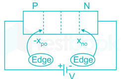
A forward-biased p-n homojunction diode is shown below:

The maximum recombination rate (Umax) is given by:

Umax=12niVTHσ0e(V/2VT).Nt{U_{max}} = \frac{1}{2}{n_i}{V_{TH}}{\sigma _0}{{\rm{e}}^{\left( {V/2{V_T}} \right)}}.{N_t}

Where,

ni: intrinsic concentration.

VTH: thermal velocity of carriers.

σ­0 = Capture cross-section.

V: applied forward voltage.

VT: Thermal voltage.

Nt: probability density of energy state Et which is present between EC and Ev

Observations:

  • Umax ∝ ni, so option 1 is correct.
  • Maximum recombination (Umax) occurs at the center of the depletion region. ∴ Option 2 is wrong.
  • Umax ∝ eV, ∴ Option 3 is correct.
  • Umax ∝ VTH, ∴ Option 4 is correct.
18

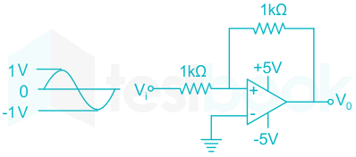
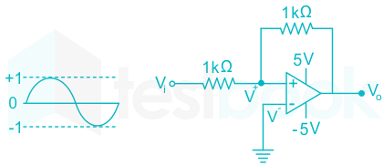
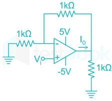
The components in the circuit shown below are ideal. If the op-amp is in positive feedback and the input voltage Vi is a sine wave of amplitude 1 V, the output voltage V0 is

  1. ((a))

    a non-inverted sine wave of 2 V amplitude

  2. ((b))

    an inverted sine wave of 1 V amplitude

  3. ((c))

    a square wave of 5 V amplitude

  4. ((d))

    a constant of either +5 V or -5 V.

Show Answer
Answer: ((d))

a constant of either +5 V or -5 V.

Analysis:

The given circuit is a Schmitt trigger circuit. It is redrawn as:

Applying KCL at the non-investing terminal, we get:

V+Vi1k+V+V01kΩ=0\frac{{{V^ + } - {V_i}}}{{1k}} + \frac{{{V^ + } - {V_0}}}{{1k{\rm{\Omega }}}} = 0

V+ - Vi + V+ - V0 = 0

V+=Vi+V02{V^ + } = \frac{{{V_i} + {V_0}}}{2}      ---(1)

Case 1:

When V0 = 5V (+Vsat)

From equation (1), we can write:

V+=5+V02=2.5+V02{V^ + } = \frac{{5 + {V_0}}}{2} = 2.5 + \frac{{{V_0}}}{2}

For a positive peak of +1V for Vi, V+ will be:

V+ = 2.5 + 0.5

V+ = 3V

Since V- = 0 V

The difference in the non-inverting and inverting terminal of Op-Amp is:

Vd = V+ - V-

Vd = 3 V

Since the Op-Amp amplifies the difference in the input voltage, the output will remain constant at +Vsat (5V) as Vd = + 3V (Positive)

Now for a negative peak of -1V for Vin, V+ will be:

V+ = 2.5 – 0.5

V+ = 2V

Vd = 2 – 0

Vd = 2V

The difference is positive for both the positive and negative peak of Vi,

∴ The output will remain at + 5V (+Vsat), irrespective of the input.

Case 2:

When V0 = -5V (-Vsat)

Again apply KCL at the non-investing terminal, we get:

V+(5)1k+V+Vi1k=0\frac{{{V^ + } - \left( { - 5} \right)}}{{1k}} + \frac{{{V^ + } - {V_i}}}{{1k}} = 0

V+=Vi52{V^ + } = \frac{{{V_i} - 5}}{2}

V+=;2.5+Vi2{V^ + } = ; - 2.5 + \frac{{{V_i}}}{2}

Now, for a positive peak of Vi at 1V, V+ will be:

V+ = -2.5 + 0.5

V+ = -2V

Vd = V+ - V-

Vd = -2V

Since the difference is negative, the output will remain at -Vsat

Similarly, for a negative peak of Vi at -1V, V+, will be,

V+ = -2.5 – 0.5

V+ = -3V

Vd = -3V

Source the difference is negative the output will remain at -Vsat

∴ We can conclude that the output will either be +Vsat or -Vsat

19

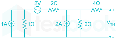
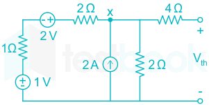
In the circuit shown below, the Thevenin voltage VTH is

  1. ((a))

    2.4 V

  2. ((b))

    2.8 V

  3. ((c))

    3.6 V

  4. ((d))

    4.5 V

Show Answer
Answer: ((c))

3.6 V

Concept:

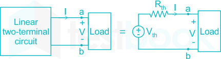
According to Thevenin’s theorem, any linear circuit across a load can be replaced by an equivalent circuit consisting of a voltage source Vth in series with a resistor Rth as shown:

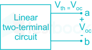
Vth = Open circuit Voltage at a – b (by removing the load), i.e.

Application:

Since Vth is simply the open-circuit voltage, we use the substitution theorem to simplify the circuit as shown:

Let Vx be Node Voltage

Applying KCL at node x, we get:

Vx2132;+Vx2=0\frac{{V_x - 2 - 1}}{3} - 2; + \frac{V_x}{2} = 0

Vx33+Vx2=2\frac{{V_x - 3}}{3} + \frac{V_x}{2} = 2

2Vx – 6 + 3Vx = 12

5Vx = 18

Vx=18/5=3.6VV_x=18/5=3.6 V

Since no current flows through the 4Ω resistance, we can write:

Vx = Vth

∴ Vth = 3.6 V

20

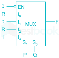
The figure below shows a multiplexer where S1 and S0 are the select lines, I0 to I3 are the input data lines, EN is the enable line, and F(P, Q, R) is the output. F is

  1. ((a))

    PQ + Q̅R 

  2. ((b))

    P + QR̅

  3. ((c))

    PQ̅R + P̅Q

  4. ((d))

    Q̅ + PR

Show Answer
Answer: ((a))

PQ + Q̅R 

Concept:

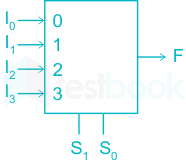
For a general 4 to 1 multiplier as shown, the output expression is written as:

F = S̅10I0 + S̅1S0I1 + S10I2 + S1S0I3  

i.e. I0 will be the output when the select inputs are 00, I1 will be the output when the select Inputs are 01, and so on.

Application:

For the given MUX, the enable input is activated (Active low enable).

∴ The output expression will be:

F = P̅Q̅R + P̅Q(0) + PQ̅R + PQ(1)

F = P̅Q̅R  + PQ̅R + PQ

F = Q̅R(P + P̅) + PQ

F = Q̅R + PQ

21

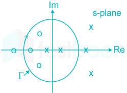
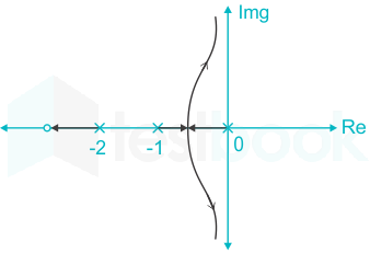
The pole-zero map of a rational function G(s) is shown below. When the closed contour Γ is mapped into the G(s)-plane, then the mapping encircles

  1. ((a))

    the origin of the G(s)-plane once in the counter-clockwise direction

  2. ((b))

    the origin of the G(s)-plane once in the clockwise direction

  3. ((c))

    the point -1 + j0 of the G(s)-plane once in the counter-clockwise direction

  4. ((d))

    the point -1+ j0 of the G(s)-plane once in the clockwise direction

Show Answer
Answer: ((b))

the origin of the G(s)-plane once in the clockwise direction

Concept:

Cauchy principles argument states that the closed contour Γ is mapped into the G(s)-plane will encircle the origin as many times as the difference between the number of poles (P) and zeros (Z) of the open-loop transfer function G(s) that are encircled by the S – plane locus Γ, i.e.

No. of encirclement is given by:

N = P – Z

Calculation:

The closed contour Γ of a pole-zero map of a rational function G(s) contains 2 poles and 3 zeros.

So, the number of encirclement will be:

N = P – Z

N = 2 – 3 = -1

Hence,

It encircles the origin once in the clockwise direction.

Another method to solve:

The closed contour Γ of a pole-zero map of a rational function G(s) is encircling 2 poles and 3 zeros in a clockwise direction, hence the corresponding G(s) plane contour encircles origin 2 times in anti-clockwise direction and 3 times in clockwise direction.

Hence, Effectively it encircles origin once in the clockwise direction.

Special note:

  • If we discuss the stability of the open-loop transfer function then we take encirclement around the origin.
  • If we discuss the stability of closed-loop transfer function then we take encirclement around

 -1 + j0. (∴ Option 3 and 4 are incorrect)

22

A digital communication system transmits a block of N bits. The probability of error in decoding a bit is α. The error event of each bit is independent of the error events of the other bits. The received block is declared erroneous if at least one of its bits is decoded wrongly. The probability that the received block is erroneous is

  1. ((a))

    N(1 - α)

  2. ((b))

    αN

  3. ((c))

    1 - αN

  4. ((d))

    1 – (1 - α)N

Show Answer
Answer: ((d))

1 – (1 - α)N

Concept:

Size of the block = N bits

The received block will be erroneous when any one of the bit is wrongly detected.

Application:

Since all the bits are independent of each other, the probability that all the bits are received

correctly (PC) will be:

PC=(1α)1×(1α)2×(1α)N{P_C} = {\left( {1 - \alpha } \right)_1} \times {\left( {1 - \alpha } \right)_2} \times \ldots {\left( {1 - \alpha } \right)_N}

PC = (1 - α)N

where α is the probability of error in detection.

Now, the probability that the received block is erroneous will be:

Pe = 1 – PC

Pe = 1 – (1 - α)N

23

The impedances Z = jX, for all X in the range (-∞, ∞), map to the Smith chart as

  1. ((a))

    a circle of radius 1 with center at (0, 0).

  2. ((b))

    a point at the center of the chart

  3. ((c))

    a line passing through the center of the chart

  4. ((d))

    a circle of radius 0.5 with center at (0.5 0)

Show Answer
Answer: ((a))

a circle of radius 1 with center at (0, 0).

Concept:

For drawing a smith chart:

First, we calculate normalized impedance (z)

ZLZO=R+jX\frac{{{Z_L}}}{{{Z_O}}} = R + jX     …1)

Then we solve for constant R circles and constant X-circles by using the following formulas:

Const. R circles:

(ΓRRR+1)2+ΓI2=(1R+1)2{\left( {{{\rm{\Gamma }}_R} - \frac{R}{{R + 1}}} \right)^2} + {\rm{\Gamma }}_I^2 = {\left( {\frac{1}{{R + 1}}} \right)^2}     …2)

Const. X circles:

(ΓR1)2+[ΓI1x]2=[1x]2{\left( {{{\rm{\Gamma }}_R} - 1} \right)^2} + {\left[ {{{\rm{\Gamma }}_I} - \frac{1}{x}} \right]^2} = {\left[ {\frac{1}{x}} \right]^2}     …3)

Where, ΓR = Real part of reflection coefficients.

ΓI = Imaj part of reflection coefficients.

Calculation:

Given: Z = j X

Compare this with equation (1), we can write:

R = 0

After putting this value in equation (2), we get:

R)2 + (ΓI)2 = 1     …4)

Equation (4) represents the equation of a unit circle with center (0, 0). Hence option (1) is correct.

24

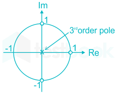
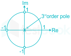
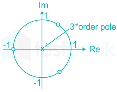
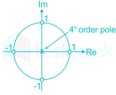
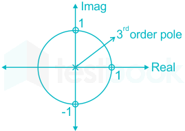
Which one of the following pole-zero plots corresponds to the transfer function of an LTI system characterized by the input-output difference equation given below?

\(y\left[ n \right] = \mathop \sum \limits_{k = 0}^3 {\left( { - 1} \right)^k}x\left[ {n - k} \right]\)

  1. ((a))

  2. ((b))

  3. ((c))

  4. ((d))

Show Answer
Answer: ((a))

Concept:

To determine Pole-zero plot, we have to first find the transfer function of LTI System, i.e.

H(z)=Y(z)X(z)H\left( z \right) = \frac{{Y\left( z \right)}}{{X\left( z \right)}}

Calculation:

Input-output difference equation is given as:

\(y\left( n \right) = \mathop \sum \limits_{K = 0}^3 {\left( { - 1} \right)^k}x\left( {n - K} \right)\)

y[n] can be represented as:

y(n) = x(n) – x(n - 1) + x(n - 2) – x(n - 3)

Taking the Z-transform, we get:

Y(z) = X(z) – z-1 X(z) + z-2 X(z) – z-3 X(z)

H(z)=Y(z)X(z)=1z1+z2z3H\left( z \right) = \frac{{Y\left( z \right)}}{{X\left( z \right)}} = 1 - {z^{ - 1}} + {z^{ - 2}} - {z^{ - 3}}

H(z)=z3z2+z1z3=(z1)(z2+1)z3H\left( z \right) = \frac{{{z^3} - {z^2} + z - 1}}{{{z^3}}} = \frac{{\left( {z - 1} \right)\left( {{z^2} + 1} \right)}}{{{z^3}}}

Hence, Pole-zero plot is:

25

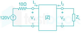
In the given circuit, the two-point network has the impedance matrix \(\left[ Z \right] = \left[ {\begin{array}{*{20}{c}} {40}&{60}\ {60}&{120} \end{array}} \right]\). The value of ZL for which maximum power is transferred to the load is _______ Ω. 

26

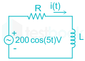
The current in the RL-circuit shown below is i(t) = 10 cos (5t – π/4) A. The value of the inductor (rounded off to two decimal places) is ______ H

27

In the circuit shown below, all the components are ideal and the input voltage is sinusoidal. The magnitude of the steady-state output V0 (rounded off to two decimal places) is ______ V.

28

In the circuit shown below, all the components are ideal. If Vi is +2 V, the current I0 sourced by the op-amp is ______ mA

29

In an 8085 microprocessor, the number of address lines required to access a 16 K byte memory bank is

30

A 10-bit D/A converter is calibrated over the full range from 0 to 10 V. If the input to the D/A converter is 13A (in hex), the output (rounded off to three decimal places) is ______V

31

A transmission line of length 3λ/4 and having a characteristic impedance of 50 Ω is terminated with a load of 400 Ω. The impedance (rounded off to two decimal places) seen at the input end of the transmission line is ______ Ω

32

A binary random variable X takes the value +2 or -2. The probability P(X = +2) = α. The value of α (rounded off to one decimal place), for which the entropy of X is maximum, is

33

The loop transfer function of a negative feedback system is

G(s)H(s)=K(s+11)s(s+2)(s+8)G\left( s \right)H\left( s \right) = \frac{{K\left( {s + 11} \right)}}{{s\left( {s + 2} \right)\left( {s + 8} \right)}}

The value of K, for which the system is marginally stable, is

34

The random variable

\(Y = \mathop \smallint \limits_{ - \infty }^\infty W\left( t \right)\phi \left( t \right)dt,\) where

\(\phi \left( t \right)=;\left{ {\begin{array}{*{20}{c}} {1;}&{5 \le t \le 7}\ {0;}&{Otherwise} \end{array}} \right}\)

And W(t) is a real white Gaussian noise process with two-sided power spectral density S(f) = 3 W/Hz, for all f. The variance of Y is:

35

The two sides of a fair coin are labeled as 0 and 1. The coin is tossed two times independently. Let M and N denote the labels corresponding to the outcomes of those tosses. For a random variable X, defined as X = min (M, N), the expected value E(X) (rounded off to two decimal places) is _______

36

Consider the following system of linear equations,

x1 + 2x2 = b1 

2x1 + 4x2 = b2 

3x1 + 7x2 = b3 

3x1 + 9x2 = b4 

Which one of the following conditions ensures that a solution exists for the above system?

  1. ((a))

    b2 = 2b1 and 6b1 – 3b3 + b4 = 0

  2. ((b))

    b3 = 2b1 and 6b1 – 3b3 + b4 = 0

  3. ((c))

    b2 = 2b1 and 3b1 – 6b3 + b4 = 0

  4. ((d))

    b3 = 2b1 and 3b1 – 6b3 + b4 = 0

Show Answer
Answer: ((a))

b2 = 2b1 and 6b1 – 3b3 + b4 = 0

Given:

x1 + 2x2 = b1 ....1)

2x1 + 4x2 = b2  ....2)

3x1 + 7x2 = b3  ....3)

3x1 + 9x2 = b4  ....4)

 From equations (1) and (2), it is clear that:

b2 = 2b1

So options (2) and (4) are incorrect.

Evaluating option (3) now, we are given:

3b1 – 6b3 + b 4 = 0

Using Equation 1, 3 and 4, we can write:

3(x1 + 2x2) - 6(3x1 + 7x2) + 3x1 + 9x2 ≠ 0

Hence option 3 is also incorrect.

Analysing option 1, we are given:

6b1 – 3b3 + b4 = 0

Put the value from equation 1, 3 and 4

6(x1 + 2x2) - 3(3x1 + 7x2) + 3x1 + 9x2 = 0


ence option 1 is correct.

37

Which one of the following options contains two solutions of the differential equation dydx=(y1)x?\frac{{dy}}{{dx}} = \left( {y - 1} \right)x?

  1. ((a))

    In |y - 1| = 0.5 x2 + C and y = 1

  2. ((b))

    In {y - 1} = 2x2 + C and y = 1

  3. ((c))

    In |y - 1| = 0.5 x2 + C and y = -1

  4. ((d))

    In |y - 1| = 2x2 + C and y = -1

Show Answer
Answer: ((a))

In |y - 1| = 0.5 x2 + C and y = 1

dydx=(y1)x\frac{{dy}}{{dx}} = \left( {y - 1} \right)x     ---(1)

The given equation can be solved using the variable separable method as:

dyy1=x;dx\frac{{dy}}{{y - 1}} = x;dx

Integrating both sides, we get:

dyy1=x;dx\smallint \frac{{dy}}{{y - 1}} = \smallint x;dx

ln;(y1)=x22+Cln;\left( {y - 1} \right) = \frac{{{x^2}}}{2} + C     ---(2)

Now, from equation (1), we get:

dydx=0\frac{{dy}}{{dx}} = 0 for y = 1

∴ y = constant = 1 is also a solution to the given differential equation.

38

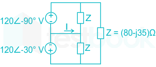
The current I in the given network is

  1. ((a))

    0 A

  2. ((b))

    2.38 ∠ - 96.37° A 

  3. ((c))

    2.38 ∠ 143.63° A

  4. ((d))

    2.38 ∠ -23.63°A 

Show Answer
Answer: ((c))

2.38 ∠ 143.63° A

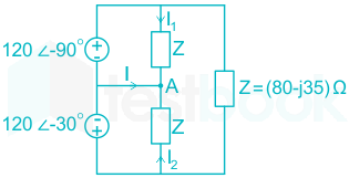
Since the voltage sources are in parallel with Z, I1 and I2 will be calculated as:

I1=12090Z{I_1} = \frac{{120\angle - 90^\circ }}{Z} 

Z = 80 – j35

In polar form, this can be written as:

Z = 87.32 ∠-23.63

I1=1209087.3223.63{I_1} = \frac{{120\angle 90^\circ }}{{87.32\angle - 23.63}}

I1 = 1.374 ∠-90 + 23.63°

I1 = 1.374 ∠-66.37°

Similarly,

I2=1203087.3223.63{I_2} = \frac{{120\angle - 30^\circ }}{{87.32\angle - 23.63}} 

I2 = 1.374 ∠-6.37°

Applying KCL at node A, we get:

I + I1 + I2 = 0

I = -(I1 + I2)

I = -(1.374 < -66.37 + 1.374 ∠-6.37°)

Converting back to coordinate axis:

I = -(0.55 – 1.258 j + 1.365 – 0.252 j)

I = (2.915 – 1.41 j)

I = -2.915 + 1.47 j

I=(1.916)2+(1.41)2tan1(1.411.915)I = \sqrt {{{\left( { - 1.916} \right)}^2} + {{\left( {1.41} \right)}^2}} \angle {\tan ^{ - 1}}\left( {\frac{{1.41}}{{ - 1.915}}} \right)

I = 2.38 ∠-36.36

I = 2.38 ∠180 – 36.36

I = 2.38 ∠143.63

39

A finite duration discrete-time signal x[n] is obtained by sampling the continuous-time signal x(t) = cos (200πt) at sampling instants t = n/400, n = 0, 1, …, 7. The 8-point discrete Fourier transform (DFT) of x[n] is defined as:

\(X\left[ k \right] = \mathop \sum \limits_{n = 0}^7 x\left[ n \right]{e^{ - j\frac{{\pi kn}}{4}}},;k = 0,;1,; \ldots ,;7.\)

Which one of the following statements is TRUE?

  1. ((a))

    All X[k] are non-zero

  2. ((b))

    Only X[4] is non-zero

  3. ((c))

    Only X[2] and X[6] are non-zero

  4. ((d))

    Only X[3] and X[5] are non-zero

Show Answer
Answer: ((c))

Only X[2] and X[6] are non-zero

Concept:

Sampling theorem is the bridge between continuous-time signals and discrete-time signals i.e., we convert continuous signals to discrete signals using sampling theorem.

y[n]= x(nTs)

Ts = Sampling interval

Calculation:

It is given that a finite duration discrete signal x(n) is obtained by sampling x(t) = cos(200πt) with Ts = n/400

x(t) = cos 200 π t

Since the sampling instant is t = n/400, x(t) can be written as:

x(n)=cos[200πn400]x\left( n \right) = \cos \left[ {200\pi \cdot \frac{n}{{400}}} \right]

x(n)=cos(π2n)x\left( n \right) = \cos \left( {\frac{\pi }{2}n} \right) n = 0, 1, 2 …7

\(x\left( n \right) = \left{ {\cos 0,;\cos \frac{\pi }{2},\cos \pi ,\cos \frac{{3\pi }}{2}, \ldots ,\cos \frac{{7\pi }}{2}} \right}\)

x(n) = {+1, 0, -1, 0, +1, 0, -1, 0}

The discrete Fourier Transform of x[n] will be X[k].

Assuming, y(n) = [1, -1, 1, -1], i.e.

x(n)=y(n2)x\left( n \right) = y\left( {\frac{n}{2}} \right)

Then its 4-point DFT will be:

\(Y\left( K \right) = \left[ {\begin{array}{{20}{c}} 1&1&1&1\ 1&{ - j}&{ - 1}&j\ 1&{ - 1}&1&{ - 1}\ 1&j&{ - 1}&{ - j} \end{array}} \right]\left[ {\begin{array}{{20}{c}} 1\ { - 1}\ 1\ { - 1} \end{array}} \right]\)

After solving we’ll get,

Y(K) \( = \left[ {\begin{array}{*{20}{c}} 0&0&4&0 \end{array}} \right]\)

We know that,

If y(n) ↔ Y(K)

Then y(nm)y\left( {\frac{n}{m}} \right) ↔ [Y(K), Y(K), Y(K) … m times]

So, y(n2)y\left( {\frac{n}{2}} \right) ↔ [Y(K), Y(K)]

Since, Y(K) = [0, 0, 4, 0]

\(x\left( n \right) = y\left( {\frac{n}{2}} \right) \leftrightarrow \left[ {\begin{array}{*{20}{c}} {0,}&{0,}&{\underbrace {4,}{X(2)}}&{0,}&{0,}&{0,}&{\underbrace {4,}{X(6)}}&0 \end{array}} \right]\)

So, only X(2) & X(6) are non zero.

40

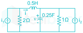
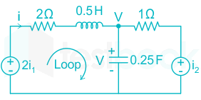
For the given circuit, which one of the following is the correct state equation?

  1. ((a))

    \(\frac{d}{{dt}}\left[ {\begin{array}{{20}{c}} v\ i \end{array}} \right] = \left[ {\begin{array}{{20}{c}} { - 4}&4\ { - 2}&{ - 4} \end{array}} \right]\left[ {\begin{array}{{20}{c}} v\ i \end{array}} \right] + \left[ {\begin{array}{{20}{c}} 0&4\ 4&0 \end{array}} \right]\left[ {\begin{array}{*{20}{c}} {{i_1}}\ {{i_2}} \end{array}} \right]\)

  2. ((b))

    \(\frac{d}{{dt}}\left[ {\begin{array}{{20}{c}} v\ i \end{array}} \right] = \left[ {\begin{array}{{20}{c}} { - 4}&{ - 4}\ { - 2}&4 \end{array}} \right]\left[ {\begin{array}{{20}{c}} v\ i \end{array}} \right] + \left[ {\begin{array}{{20}{c}} 4&4\ 4&0 \end{array}} \right]\left[ {\begin{array}{*{20}{c}} {{i_1}}\ {{i_2}} \end{array}} \right]\)

  3. ((c))

    \(\frac{d}{{dt}}\left[ {\begin{array}{{20}{c}} v\ i \end{array}} \right] = \left[ {\begin{array}{{20}{c}} 4&{ - 4}\ { - 2}&{ - 4} \end{array}} \right]\left[ {\begin{array}{{20}{c}} v\ i \end{array}} \right] + \left[ {\begin{array}{{20}{c}} 0&4\ 4&4 \end{array}} \right]\left[ {\begin{array}{*{20}{c}} {{i_1}}\ {{i_2}} \end{array}} \right]\)

  4. ((d))

    \(\frac{d}{{dt}}\left[ {\begin{array}{{20}{c}} v\ i \end{array}} \right] = \left[ {\begin{array}{{20}{c}} { - 4}&{ - 4}\ { - 2}&{ - 4} \end{array}} \right]\left[ {\begin{array}{{20}{c}} v\ i \end{array}} \right] + \left[ {\begin{array}{{20}{c}} 4&0\ 0&4 \end{array}} \right]\left[ {\begin{array}{*{20}{c}} {{i_1}}\ {{i_2}} \end{array}} \right]\)

Show Answer
Answer: ((a))

\(\frac{d}{{dt}}\left[ {\begin{array}{{20}{c}} v\ i \end{array}} \right] = \left[ {\begin{array}{{20}{c}} { - 4}&4\ { - 2}&{ - 4} \end{array}} \right]\left[ {\begin{array}{{20}{c}} v\ i \end{array}} \right] + \left[ {\begin{array}{{20}{c}} 0&4\ 4&0 \end{array}} \right]\left[ {\begin{array}{*{20}{c}} {{i_1}}\ {{i_2}} \end{array}} \right]\)

After applying source transformation, the circuit is redrawn as:

Applying KVL for the given loop, we get:

2i12i0.5didtV=02{i_1} - 2i - 0.5\frac{{di}}{{dt}} - V = 0

0.5didt=2i12iV0.5\frac{{di}}{{dt}} = 2{i_1} - 2i - V

didt=4i2V+4i1\frac{{di}}{{dt}} = - 4i - 2V + 4{i_1}       ---(1)

Applying KCL at node V, we get:

i=0.25dVdt+Vi21i = 0.25\frac{{dV}}{{dt}} + \frac{{V - {i_2}}}{1}

14dVdt=i+i2V\frac{1}{4}\frac{{dV}}{{dt}} = i + {i_2} - V

dVdt=4V+4i+4i2\frac{{dV}}{{dt}} = - 4V + 4i + 4{i_2}     ---(2)

In Matrix from, equation (1) and (2) can be written as:

\(\frac{d}{{dt}}\left[ {\begin{array}{{20}{c}} V\ i \end{array}} \right] = \left[ {\begin{array}{{20}{c}} { - 4}&4\ { - 2}&{ - 4} \end{array}} \right]\left[ {\begin{array}{{20}{c}} V\ i \end{array}} \right] + \left[ {\begin{array}{{20}{c}} 0&4\ 4&0 \end{array}} \right]\left[ {\begin{array}{*{20}{c}} {{i_1}}\ {{i_2}} \end{array}} \right]\)

41

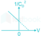
A one-sided abrupt pn junction diode has a depletion capacitance CD of 50 pF at a reverse bias of 0.2 V. The plot of 1CD2\frac{1}{{C_D^2}} versus the applied voltage V for this diode is a straight line as shown in the figure below. The slope of the plot is ______ × 1020 F-2V-1

  1. ((a))

    -5.7

  2. ((b))

    -3.8

  3. ((c))

    -1.2

  4. ((d))

    Data insufficient

Show Answer
Answer: ((d))

Data insufficient

Concept:

Depletion capacitance is calculated as:

CD=εAW{C_D} = \frac{{\varepsilon A}}{W}    ---(1)

W = Width of the depletion region given by:

W=[[2εq(1NA+1ND)](VbiV)]1/2W = {\left[ {\left[ {\frac{{2\varepsilon }}{q}\left( {\frac{1}{{{N_A}}} + \frac{1}{{{N_D}}}} \right)} \right]\left( {{V_{bi}} - V} \right)} \right]^{1/2}}      ---(2)

Vbi = built-in potential

V = Anode to cathode applied potential

Calculation:

Given: CD = 50 pF, V = 0.2 V

From equation 2) & equation 1)

CD=εA[2εq(1NA+1ND)(VbiV)]1/2{C_D} = \frac{{\varepsilon A}}{{{{\left[ {\frac{{2\varepsilon }}{q}\left( {\frac{1}{{{N_A}}} + \frac{1}{{{N_D}}}} \right)\left( {{V_{bi}} - V} \right)} \right]}^{1/2}}}}

CD=K(VbiV)1/2{C_D} = \frac{K}{{{{\left( {{V_{bi}} - V} \right)}^{1/2}}}}

K=εA2εq(1NA+1ND)K = \frac{{\varepsilon A}}{{\sqrt {\frac{{2\varepsilon }}{q}\left( {\frac{1}{{{N_A}}} + \frac{1}{{{N_D}}}} \right)} }}

1CD2=1K2(VbiV)\frac{1}{{{C_{{D^2}}}}} = \frac{1}{{{K^2}}}\left( {{V_{bi}} - V} \right)       ---(3)

1CD2=m(VbiV)\because \frac{1}{{{C_{{D^2}}}}} = m\left( {{V_{bi}} - V} \right)

Comparing this with y = mx + c, we can write:

Slope (m) =1K2= \frac{1}{{{K^2}}}    

Putting the respective values, we get:

1(50×1012)2=m(Vbi0.2)\frac{1}{{{{\left( {50 \times {{10}^{ - 12}}} \right)}^2}}} = m\left( {{V_{bi}} - 0.2} \right)

Hence, m=10242500(Vbi0.2)m = \frac{{{{10}^{24}}}}{{2500\left( {{V_{bi}} - 0.2} \right)}}

We need Vbi to find the slope of the plot, Vbi is not given so the data is insufficient and it cannot be determined.

42

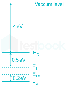
The band diagram of a p-type semiconductor with a band-gap of 1 eV is shown. Using this semiconductor, a MOS capacitor having VTH of -0.16 V, CoxC_{ox}' of 100 nF/cm2, and a metal function of 3.87 eV is fabricated. There is no charge within the oxide. If the voltage across the capacitor is VTH, the magnitude of depletion charge per unit area (in C/cm2) is

  1. ((a))

    1.70 × 10⁻⁸

  2. ((b))

    0.52 × 10⁻⁸

  3. ((c))

    1.41 × 10⁻⁸

  4. ((d))

    0.93 × 10⁻⁸

Show Answer
Answer: ((a))

1.70 × 10⁻⁸

Concept:

The Threshold voltage for a capacitor is calculated as:

\({V_T} = {\phi {ms}} - \frac{{{Q{ox}}}}{{{C_{ox}}}} - \frac{{Q_d'}}{{{C_{ox}}}} + 2{\phi _{fp}}\)        ---(1)

ϕms = Metal – semiconductor work function difference

Qox = Oxide charge

Qd’ = Depletion charge per unit area

Con = Oxide capacitance

ϕfp = Energy gap between the intrinsic gap and the Fermi level.

Application:

Given: ϕms = 3.87 eV

ϕs = Energy required to move an electron from the semiconductor Fermi level to the vaccum.

From the given Energy-bad diagram, we get:

ϕs = 4 eV + (1 – 0.2) eV

ϕs = 4.8 eV

∴ ϕms = 3.87 eV – 4.8 eV

ϕms = -0.93 eV

ϕfp = Ei - Efs

ϕfp = (1 – 0.5 – 0.2) eV

ϕfp = 0.3 eV

Also, as there is no-charge within the oxide, Qox = 0

Substituting these values in equation (1), we get:

0.16=0.93;eVQd(100);×;109+2;(0.3;eV)0.16 = - 0.93;eV - \frac{{Q_d'}}{{\left( {100} \right); \times ;{{10}^{ - 9}}}} + 2;\left( {0.3;eV} \right)

Qd100;×;109=;0.17\frac{{Q_d'}}{{100; \times ;{{10}^{ - 9}}}} = ; - 0.17

Qd=;1.7×10⁸;C/cm2Q_d' = ; - 1.7 \times {10^{ - 8}};C/c{m^2}

∴ The magnitude of depletion charge per unit area will be 1.7 × 10⁻⁸ C/m2

43

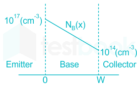
The base of an npn BJT T1 has a linear doping profile NB (x) as shown below.

The base of another npn BJT T2 has a uniform doping NB of 1017 cm-3. All other parameters are identical for both devices. Assuming that the hole density profile is the same as that of doping, the common-emitter current gain of T1 is

  1. ((a))

    approximately 2.0 times that of T2

  2. ((b))

    approximately 0.3 times that of T2

  3. ((c))

    approximately 2.5 times that of T2

  4. ((d))

    approximately 0.7 times that of T2

Show Answer
Answer: ((a))

approximately 2.0 times that of T2

Concept:

  • ​The doping concentration at the base affects the emitter gain (β), i.e. β is dependent on the doping concentration.
  • If the doping at the base increases, the recombination of the carriers from the emitter region increases. This reduces the emitter current gain, as fewer carriers from the emitter finally reach the collector.
  • Similarly, less the doping concentration at the base, less will be the recombination of the carriers at the base and more carriers will reach the collector resulting in more emitter gain.


Mathematically this can be written as:

β1Base Doping\beta \propto\frac{1}{Base~Doping}

Analysis:

For transistor T1, we can write:

β1NB1\beta \propto\frac{1}{N_{B1}}   ---(1)

For transistor T2, we can write:

β21NB2\beta_2\propto\frac{1}{N_{B2}}   ---(2)

Dividing both the equations, we get:

β1β2=NB2NB1\frac{\beta_1}{\beta_2}=\frac{N_{B2}}{N_{B1}}   ---(3)

NB = Net concentration at the base also called the dose.

NB=(Doping Concentration)dxN_B=∫(Doping~ Concentration)dx

Calculation:

For transistor T1, we get:

\({N_{B1}} = \mathop \smallint \limits_0^W {N_{B1}}\left( x \right)dx\)

From the given doping profile, we get:

NB1(x)=(101710140W)x+NB1(0){N_{B1}}\left( x \right) = \left( {\frac{{{{10}^{17}} - {{10}^{14}}}}{{0 - W}}} \right)x + {N_{B1}}\left( 0 \right)

NB1(x)(1017W)x+1017{N_{B1}}\left( x \right) \approx \left( { - \frac{{{{10}^{17}}}}{W}} \right)x + {10^{17}}

The net concentration or dose at the base of transistor T2 will be:

\({N_{B2}} = \mathop \smallint \nolimits \left( {\left( { - \frac{{{{10}^{17}}}}{W}} \right)x + {{10}^{17}}} \right)dx\)

\({N_{B2}} = \mathop \smallint \nolimits \left( {\left( { - \frac{{{{10}^{17}}}}{W}} \right)\left( {\frac{{{x^2}}}{2}} \right) + {{10}^{17}}x} \right)_0^W\)

NB2=(1017W)(W22)+1017W{N_{B2}} = \left( { - \frac{{{{10}^{17}}}}{W}} \right)\left( {\frac{{{W^2}}}{2}} \right) + {10^{17}}W

NB2=1017W10172W{N_{B2}} = {10^{17}}W - \frac{{{{10}^{17}}}}{2}W

NB2=10172W{N_{B2}} = \frac{{{{10}^{17}}}}{2}W

The ratio of the two emitter gains, using Equation (3) will be:

β1β2=1017W1017W2\frac{{{\beta _1}}}{{{\beta _2}}} = \frac{{{{10}^{17}}W}}{{\frac{{{{10}^{17}}W}}{2}}}

β1β2=2\frac{{{\beta _1}}}{{{\beta _2}}} = 2

β1 = 2 β2

44

A pn junction solar cell of area 1.0 cm2, illuminated uniformly with 100 mW cm-2, has the following parameters: Efficiency = 15%, open circuit voltage = 0.7 V, fill factor = 0.8, and thickness = 200 μm. The charge of an electron is 1.6 × 10⁻¹⁹ C. The average optical generation rate (in cm-3s-1) is

  1. ((a))

    0.84 × 10¹⁹

  2. ((b))

    5.57 × 10¹⁹

  3. ((c))

    1.04 × 10¹⁹

  4. ((d))

    83.60 × 10¹⁹

Show Answer
Answer: ((a))

0.84 × 10¹⁹

Concept:

The fill factor of a solar cell is defined as:

FF=PoutVoc;×;IscFF = \frac{{{P_{out}}}}{{{V_{oc}}; \times ;{I_{sc}}}}

Voc = Open-circuit voltage

Pout = FF × Voc × Isc

Efficiency is the ratio of the output power to the input power, i.e.,

η=PoutPin\eta = \frac{{{P_{out}}}}{{{P_{in}}}}

η=F.F;×;Voc;×;IscPin\eta = \frac{{F.F; \times; {V_{oc}}; \times ;{I_{sc}}}}{{{P_{in}}}}       ---(1)

Also, the optical generation rate (GL) will be:

GL=Iscq;×;Area;×;Thickness{G_L} = \frac{{{I_{sc}}}}{{q; \times ;Area; \times ;Thickness}}       ---(2)

 Calculation:

Given η = 0.25, FF = 0.8, Voc = 0.7 and thickness = 200 μm.

Pin=(100mWcm2)×(1;cm2){P_{in}} = \left( {100\frac{{mW}}{{c{m^2}}}} \right) \times \left( {1;c{m^2}} \right) 

Isc = 0.026 A

The optical generation rate (using equation (2)) will be:

GL=0.0261.6;×;1019;×;1;×;100;×;1004{G_L} = \frac{{0.026}}{{1.6; \times ;{{10}^{ - 19}}; \times ;1; \times ;100; \times ;{{100}^{ - 4}}}}

= 8.37 × 1018

= 0.837 × 1019 cm-3s-1

45

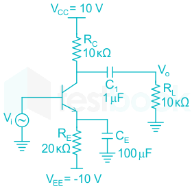
For the BJT in the amplifier shown below, VBE = 0.7 V, kT/q = 26 mV. Assume that BJT output resistance (r0) is very high and the base current is negligible. The capacitors are also assumed to be short-circuited at signal frequencies. The input Vi is direct coupled. The low-frequency voltage gain v0/vi of the amplifier is

  1. ((a))

    -89.42

  2. ((b))

    -128.21

  3. ((c))

    -178.85

  4. ((d))

    -256.42

Show Answer
Answer: ((a))

-89.42

Concept:

The small-signal (low-frequency) voltage gain of a common emitter, with bypassed emitter resistor is given by:

Av = -gm (Rc||RL)

gm = Trans conductance parameter defined as:

gm=IcVT{g_m} = \frac{{{I_c}}}{{{V_T}}}

Ic = DC collector current obtained by doing the DC analysis of the amplifier

Application:

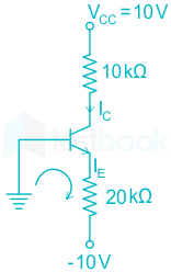
For DC analysis all the capacitor are open-circuited as shown:


Given that the base current is negligible, we can write:

Ic ≈ IE

Applying KVL for the above loop, we get:

0 - VBE - IC (20 k) + 10 = 0

IC=100.720kmA{I_C} = \frac{{10 - 0.7}}{{20k}}mA

IC = 0.465 mA

gm=IcVT=0.465;m26;m{g_m} = \frac{{{I_c}}}{{{V_T}}} = \frac{{0.465;m}}{{26;m}}

gm = 0.01788 A/V

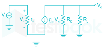
The small signal model is drawn as:

The small-signal gain will be:

Av = -gm (Rc||RL)

Putting on the respective values, we get:

Av = -(0.0178) (10k||10k)

Av = -0.0178 × 5k

Av = -89.42

46

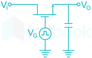
An enhancement MOSFET of threshold voltage 3 V is being used in the sample and hold circuit given below. Assume that the substrate of the MOS device is connected to – 10 V. If the input voltage VI lies between ± 10 V, the minimum and the maximum values of VG required for proper sampling and holding respectively, are

  1. ((a))

    3 V and -3 V

  2. ((b))

    10 V and – 10 V

  3. ((c))

    13 V and -7 V

  4. ((d))

    10 V and – 13 V

Show Answer
Answer: ((c))

13 V and -7 V

Concept:

Sample and hold circuit is an analog device that samples the voltage of a continuously varying signal and holds its signal value at a constant level for a specified period.

For proper sampling operation, the MOSFET should be on i.e.

VGS>VT{V_{GS}} > {V_T}

For proper holding operation, the MOSFET should be off i.e.

VGS<VT{V_{GS}} < {V_T}

Calculation:

Given: VT = 3 V, V(I)min= -10V, V(I)max = 10V

The MOSFET should be on for sampling operation, i.e.

VGS>VT{V_{GS}} > {V_T}

VGV(I)max>VT{V_G} - {V_{\left( I \right)max}} > {V_T}

VG10>3{V_G} - 10 > 3

VG>13V{V_G} > 13V 

The MOSFET should be off for holding operation, i.e.

VGS<VT{V_{GS}} < {V_T} 

VGV(I)min<VT{V_G} - {V_{\left( I \right)min}} < {V_T}

VG(10)<3{V_G} - \left( { - 10} \right) < 3

VG<7;V{V_G} < - 7;V

Hence, the minimum and the maximum values of VG required for proper sampling and holding respectively, are 13V and -7V respectively.

47

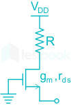
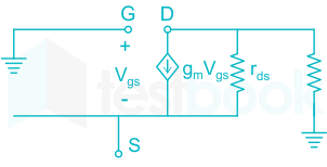
Using the incremental low-frequency small-signal model of the MOS device, the Norton equivalent resistance of the following circuit is

  1. ((a))

    rds+R+gmrdsR{r_{ds}} + R + {g_m}{r_{ds}}R

  2. ((b))

    rds+R1+gmrds\frac{{{r_{ds}} + R}}{{1 + {g_m}{r_{ds}}}}

  3. ((c))

    rds+1gm+R{r_{ds}} + \frac{1}{{{g_m}}} + R

  4. ((d))

    rds+R{r_{ds}} + R

Show Answer
Answer: ((b))

rds+R1+gmrds\frac{{{r_{ds}} + R}}{{1 + {g_m}{r_{ds}}}}

AC equivalent circuit is redrawn as:

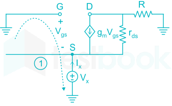
Since there is a dependent source here, we will use a test battery Vx at the source to evaluate the Norton equivalent resistance as shown:

So, RN=VxIx{R_N} = \frac{{{V_x}}}{{{I_x}}}

Applying KVL in loop 1, we get:

Vx = -Vgs

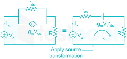
Above circuit can be replaced by:

Apply KVL we get,

-Vx + Ix (rds + R) – gmVxrds = 0

VxIx=rds;+;R1;+;gmrds=RN\frac{{{V_x}}}{{{I_x}}} = \frac{{{r_{ds}}; + ;R}}{{1; + ;{g_m}{r_{ds}}}} = {R_N}

48

P, Q, and R are the decimal integers corresponding to the 4-bit binary number 1100 considered in signed magnitude, 1’s complement, and 2’s complement representations, respectively. The 6-bit 2’s complement representation of (P + Q + R) is

  1. ((a))

    110101

  2. ((b))

    110010

  3. ((c))

    111101

  4. ((d))

    111001

Show Answer
Answer: ((a))

110101

Concept:

1. Signed magnitude representation uses the most significant bit (MSB) a sign bit.

  • If the sign bit is ‘0’ then the number is positive.
  • If the sign bit is ‘1’ then the number is negative.

The remaining bits represent the magnitude of the binary number.

2. 1’s complement representation:

It is a representation of a binary number obtained by toggling all bits in it i.e. transforming the 0 bit to 1 and the 1 bit to 0.

3. 2’s complement representation:

It is obtained by simply adding 1 to the 1’s complement of that binary number.

Calculation:

Given: 4-bit binary number = 1100

Signed magnitude representation (P): - 4

1’s complement representation (Q): - 3

2’s complement representation (R): - 4

So,

P + Q + R = (-4) + (-3) + (-4) = -11

(-11)10 is represented in 2’s complement as:

-(11)10 = 10101

Since the Options are in 6 bits so, we copy sign bit once towards left.

So 6-bit representation of (-11)10 is 110101

49

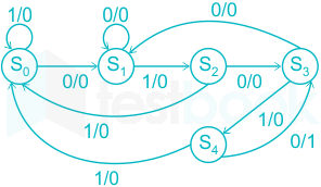
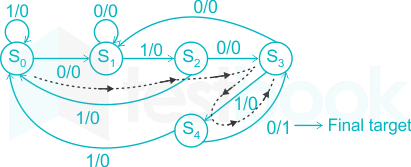
The state diagram of a sequence detector is shown below. State S0 is the initial state of the sequence detector. If the output is 1, then

  1. ((a))

    the sequence 01010 is detected

  2. ((b))

    the sequence 01011 is detected

  3. ((c))

    the sequence 01110 is detected

  4. ((d))

    the sequence 01001 is detected

Show Answer
Answer: ((a))

the sequence 01010 is detected

Concept:

In general,

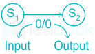
This state diagram shows that the state will transit from S1 to S2 when the Input is 0 and at the end of the transition, it will produce output as 0.

Calculation:

The state diagram of a sequence detector is given where S0 is the initial state.

If the output is 1, we then need to obtain an input sequence.

The above-dotted line shows the desired sequence to get output 1. So the state transition is as follows:

Corresponding Input sequence: 0, 1, 0, 1, 0

Corresponding Output sequence: 0, 0, 0, 0, 1

Hence, Detected Output sequence = 0 1 0 1 0.

50

The characteristic equation of a system is

s3+3s2+(K+2)s+3K=0{s^3} + 3{s^2} + \left( {K + 2} \right)s + 3K = 0

In the root locus plot for the given system, as K varies from 0 to ∞, the break-away or break-in point(s) lie within

  1. ((a))

    (-1, 0)

  2. ((b))

    (-2, -1)

  3. ((c))

    (-3, -2)

  4. ((d))

    (-∞, -3)

Show Answer
Answer: ((a))

(-1, 0)

Concept:

A  breakaway point is a point on a real axis segment of the root locus between two real poles, where the two real closed-loop poles meet and diverge to become complex conjugates.

The breakaway/ break-in/ saddle point is calculated from the solution of:

dKdS=0\frac{{dK}}{{dS}} = 0 .

Calculation:

Given:

s3+3s2+(K+2)s+3K=0{s^3} + 3{s^2} + \left( {K + 2} \right)s + 3K = 0

s3+3s2+Ks+2s+3K=0{s^3} + 3{s^2} + Ks + 2s + 3K = 0

K=(s3+3s2+2s)s+3K = \frac{{ - \left( {{s^3} + 3{s^2} + 2s} \right)}}{{s + 3}}

dKds=[(s+3)(3s2+6s+2)(s3+3s2+2s)](s+3)2=0\frac{{dK}}{{ds}} = \frac{{ - \left[ {\left( {s + 3} \right)\left( {3{s^2} + 6s + 2} \right) - \left( {{s^3} + 3{s^2} + 2s} \right)} \right]}}{{\left( {s + 3} \right)^2}} = 0

On solving we’ll get:

2s3+12s2+18s+6=02{s^3} + 12{s^2} + 18s + 6 = 0

Hence,

s=0.46,;3.87,1.65s = - 0.46,; - 3.87, - 1.65 

So, break away point lie in between (-1,0).

This is explained as shown:

Note:

Breakaway point is formed when an underdamped system is converted into an overdamped system, i.e. it is the point at which the system becomes critically stable.

51

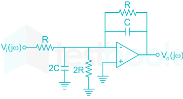
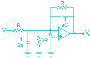
The components in the circuit given below are ideal. If R = 2 kΩ and C = 1 μF, the -3 dB cut-off frequency of the circuit in Hz is

  1. ((a))

    14.92

  2. ((b))

    34.46

  3. ((c))

    59.68

  4. ((d))

    79.58

Show Answer
Answer: ((d))

79.58

Concept:

The cut-off frequency is the frequency at which the gain is 12\frac{1}{{\sqrt 2 }} times of the maximum gain.

The given circuit is s-domain is as shown:

Applying KCL at node A, we can write:

VViR+V1/2s+V2R+VV0R+VV02/sC=0\frac{{{V^ - } - {V_i}}}{R} + \frac{{{V^ - }}}{{1/2s}} + \frac{{{V^ - }}}{{2R}} + \frac{{{V^ - } - {V_0}}}{R} + \frac{{{V^ - } - {V_0}}}{{2/sC}} = 0 

Since V+ = V- (Virtual short circuit), the above equation becomes:

ViR+0V0RV0sC=0\frac{{ - {V_i}}}{R} + 0 - \frac{{{V_0}}}{R} - {V_0}sC = 0

ViR=V0(1R+sC)\frac{{ - {V_i}}}{R} = {V_0}\left( {\frac{1}{R} + sC} \right)

ViR=V0R(1+sCR)\frac{{ - {V_i}}}{R} = \frac{{{V_0}}}{R}\left( {1 + sCR} \right)

-Vi = V0 (1 + sCR)

V0Vi=11+sCR\frac{{{V_0}}}{{{V_i}}} = \frac{{ - 1}}{{1 + sCR}}

In the frequency domain, this can be written as:

V0(jω)Vi(jω)=11+jωRC\frac{{{V_0}\left( {j\omega } \right)}}{{{V_i}\left( {j\omega } \right)}} = \frac{{ - 1}}{{1 + j\omega RC}}

V0(jω)Vi(jω)=11+j(ωω0)\frac{{{V_0}\left( {j\omega } \right)}}{{{V_i}\left( {j\omega } \right)}} = \frac{{ - 1}}{{1 + j\left( {\frac{\omega }{{{\omega _0}}}} \right)}}

Where ω0=1RC{\omega _0} = \frac{1}{{RC}}

We observe that, when ω=ω0=1RC\omega = {\omega _0} = \frac{1}{{RC}}, the magnitude of the gain becomes 12\frac{1}{{\sqrt 2 }} times the maximum gain, which is 1.

∴ ω=ω0=1RC\omega = {\omega _0} = \frac{1}{{RC}} is the cut-off frequency.

Calculation:

Given, R = 2kΩ, C = 1μF

ω0=1RC{\omega _0} = \frac{1}{{RC}}

2πf0=1RC2\pi {f_0} = \frac{1}{{RC}}

f0=12πRC{f_0} = \frac{1}{{2\pi RC}} 

=12π×2k×106 = \frac{1}{{2\pi \times 2k \times {{10}^{ - 6}}}} 

f0 ≅ 79.6 Hz

52

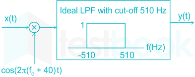
For the modulated signal x(t) = m(t) cos (2πfct), the message signal m(t) = 4 cos (1000πt) and the carrier frequency fc is 1 MHz. The signal x(t) is passed through a demodulator, as shown in the figure below. The output y(t) of the demodulator is

  1. ((a))

    cos(460πt)

  2. ((b))

    cos(920πt)

  3. ((c))

    cos(1000πt)

  4. ((d))

    cos(540πt)

Show Answer
Answer: ((b))

cos(920πt)

Concept: Low pass filter allow the low frequency components ( up to Bandwidth of filter) to pass through it.

Calculation:

x(t) = m(t) cos (2πfct)

m(t) = 4 cos (1000 πt)

The output of the multiplier(s(t)) will be:

s(t) = x(t) cos (2π(fc + 40)t)

s(t) = m(t) cos (2πfct) cos (2π(fc + 40)t)

cos(A)cos(B)=12(cos(AB)+cos(A+B))\cos \left( A \right)\cos \left( B \right) = \frac{1}{2}(\cos \left( {A - B} \right) + \cos \left( {A + B} \right))

s(t)=m(t)2[cos(2π(fcfc40)t+cos(2π(fc+fc+40)t)]s\left( t \right) = \frac{{m\left( t \right)}}{2}\left[ {\cos \left( {2\pi ({f_c} - {f_c} - 40} \right)t + \cos \left( {2\pi \left( {{f_c} + {f_c} + 40} \right)t} \right)} \right]

s(t)=m(t)2(cos(2π(40)t+cos(2π(2fc+40)t)s\left( t \right) = \frac{{m\left( t \right)}}{2}\left( {\cos \left( {2\pi \left( {40} \right)t + \cos (2\pi (2{f_c} + 40} \right)t} \right)

s(t)=4cos(1000πt)2(cos(2π40t)+cos(2π(2fc+40)t)s\left( t \right) = \frac{{4\cos \left( {1000\pi t} \right)}}{2}(\cos \left( {2\pi \cdot 40t} \right) + \cos \left( {2\pi \left( {2{f_c} + 40} \right)t} \right)

s(t) = 2 cos (100 πt)⋅cos (2π 40t) + 2 cos (1000 πt) cos (2π(2fc + 40)t

Again using the same trigonometric identify, the above equation can be written as:

s(t) = cos (1000πt – 80πt) + cos (1000πt + 80πt) + cos (1000πt – 2π(2fc + 40)t) + cos (1000πt + 2π (2fc + 40)t)

s(t) = cos (920πt) + cos (1080πt) + cos (1000πt – 2π (2fc - 40)t + cos(1000πt + 2π (2fc + 40)t)

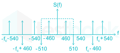
The frequency specimen of s(t) can be drawn as:

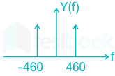
The output of the low pass filter will contain frequencies of 460 Hz only as shown:

∴ y(t) = cos (920 πt)

53

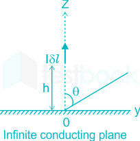
For an infinitesimally small dipole in free space, the electric field Eθ in the far-field is proportional to (e-jkr/r)sin θ, where k = 2π/λ. A vertical infinitesimally small electric dipole (δl ≪ λ) is placed at a distance h (h > 0) above an infinite ideal conducting plane, as shown in the figure. The minimum value of h, for which one of the maxima in the far-field radiation pattern occurs at θ = 60°, is

  1. ((a))

    λ

  2. ((b))

    0.5λ

  3. ((c))

    0.25λ

  4. ((d))

    0.75λ

Show Answer
Answer: ((a))

λ

Concept:

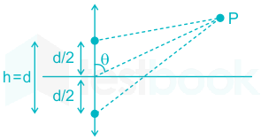
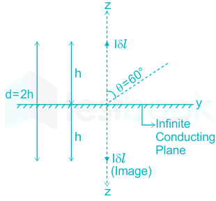
According to image theory Whenever we place a small electric dipole (δl) at a distance h (h > 0) above an infinite ideal conducting plane, the image of the small electric dipole will be formed at the same distance under the conducting plane. Thus it forms a two-element array.

For 2 element array, the array factor is given by:

A.F.=sin(NΨ2)sin(Ψ2)\left| {A.F.} \right| = \frac{{sin\left( {N\frac{\Psi }{2}} \right)}}{{\sin \left( {\frac{\Psi }{2}} \right)}}

Ψ=Kdcosθ+α\Psi = Kdcos\theta+α     ---(1)

Where,

K: 2π/λ

θ: angle from antenna array axis at point ‘p’.

Analysis:

Current phase shifts between Idl and its image is α = 0. When ever we place a dipole at height “h” above the conducting plane, there forms its image at a depth “h” below the conducting plane and thus it forms a two-element array.

For 2 element array (N = 2), the array factor will be:

A.F.=sin(NΨ2)sin(Ψ2)\left| {A.F.} \right| = \frac{{sin\left( {N\frac{\Psi }{2}} \right)}}{{\sin \left( {\frac{\Psi }{2}} \right)}}

A.F.=2sin(Ψ2)cos(Ψ2)sin(Ψ2)\left| {A.F.} \right| = \frac{{2sin\left( {\frac{\Psi }{2}} \right)cos\left( {\frac{\Psi }{2}} \right)}}{{\sin \left( {\frac{\Psi }{2}} \right)}}

A.F.=2cos(Ψ2)\left| {A.F.} \right| = 2cos\left( {\frac{\Psi }{2}} \right)

A.F.max=;2|A.F.{|_{max}} = ;2

\(\left| {A.F.{|N} = \left| {A.F.} \right|/} \right|A.F.{|{max}}\)

A.F.N=;cos(Ψ2)|A.F.{|_N} = ;cos\left( {\frac{\Psi }{2}} \right)     ---(2)

From equation 1,

Ψ=Kdcosθ+α\Psi = Kdcos\theta+α

With α = 0, and K = 2π/λ, we can write:

Ψ=2πλ.2h.cos60\Psi = \frac{{2{\rm{π }}}}{{\rm{λ }}}.2h.\cos 60

Ψ=2πλ.h\Psi = \frac{{2{\rm{π }}}}{{\rm{λ }}}.h

Put this value in equation 2 to get:

A.F.N=;cos(2π2.λ.h)|A.F.{|_N} = ;cos\left( {\frac{{2{\rm{π }}}}{{2.{\rm{λ }}}}.h} \right)

A.F.N=;cos(πλ.h)|A.F.{|_N} = ;cos\left( {\frac{{\rm{π }}}{{\rm{λ }}}.h} \right)

|A.F.|N will be maximum if the cos term in the above expression is maximum, i.e. 1. We can, therefore, write:

πλ.h=nπ\frac{{\rm{π }}}{{\rm{λ }}}.h = nπ where n = 0, 1, 2, 3....

For hmin, n = 1

πλ.h=π\frac{{\rm{π }}}{{\rm{λ }}}.h = π

h=λh = λ

54

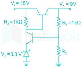
In the voltage regulator shown below, V1 is the unregulated input at 15 V. Assume VBE = 0.7 V and the base current in negligible for both the BJTs. If the regulated output V0 is 9 V, the value of R2 is _______ Ω 

55

The magnetic field of a uniform plane wave in vacuum is given by:

H(x,y,z,t)=(a^x+2a^y+ba^z)cos(ωt+3xyz)\vec H\left( {x,y,z,t} \right) = \left( {{{\hat a}_x} + 2{{\hat a}_y} + b{{\hat a}_z}} \right){\rm{cos}}\left( {\omega t + 3x - y - z} \right)

The value of b is

56

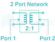
For a 2-port network consisting of an ideal lossless transformer, the parameter S21 (rounded off to two decimal places) for a reference impedance of 10 Ω, is ________.

57

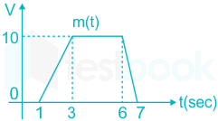
SPM(t) and SFM(t) as defined below, are the phase-modulated and the frequency-modulated waveforms, respectively, corresponding to the message signal m(t( shown in the figure.

SPM(t)=cos(1000πt+Kpm(t)){S_{PM}}\left( t \right) = {\rm{cos}}\left( {1000\pi t + {K_p}m\left( t \right)} \right) and

\({S_{FM}}\left( t \right) = {\rm{cos}}\left( {1000\pi t + {K_f}\mathop \smallint \nolimits_{ - \infty }^t m\left( \tau \right)d\tau } \right)\)

Where Kp is the phase deviation constant in radians/volt and Kf is the frequency deviation constant in radians/second/volt. If the highest instantaneous frequencies of SPM(t) and SFM(t) are the same, then the value of the ratio KpKf\frac{{{K_p}}}{{{K_f}}} is ______ seconds.

58

In a digital communication system, a symbol S randomly chosen from the set (s1, s2, s3, s4) is transmitted. It is given that s1 = -3, s2 = -1, s3 = +1 and s4 = +2. The received symbol is Y = S + W. W is a zero-mean unit-variance Gaussian random variable and is independent of S. Pi is the conditional probability of symbol error for the maximum likelihood (ML) decoding when the transmitted symbol S = si. The index i for which the conditional symbol error probability Pi is the highest is

59

A system with transfer function G(s)=1(s+1)(s+a),;a>0G\left( s \right) = \frac{1}{{\left( {s + 1} \right)\left( {s + a} \right)}},;a > 0 is subjected to an input 5 cos 3t. The steady-state output of the system is 110cos(3t1.892)\frac{1}{{\sqrt {10} }}\cos \left( {3t - 1.892} \right). The value of a is

60

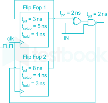
For the components in the sequential circuit shown below, tpd is the propagation delay, tsetup is the setup time, and thold is the hold time. The maximum clock frequency (rounded off to the nearest integer), at which the given circuit can operate reliably, is ______ MHz.

61

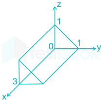
For the solid S shown below, the value of \(\iiint_{s}{xdxdy~dz}\) (rounded off to two decimal places) is ________

62

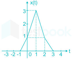
X(ω) is the Fourier transform of x(t) shown below. The value of X(ω)2dω\mathop{\int }_{-\infty }^{\infty }{{\left| X\left( \omega \right) \right|}^{2}}d\omega  (rounded off to two decimal places) is _________.

63

The transfer function of a stable discrete-time LTI system is H(z)=K(zα)z+0.5H\left( z \right) = \frac{{K\left( {z - \alpha } \right)}}{{z + 0.5}}, where K and α are real numbers. The value of α (rounded off to one decimal place) with |α| > 1, for which the magnitude response of the system is constant over all frequencies, is

64

X is a random variable with a uniform probability density function in the interval [-2, 10]. For Y = 2X – 6, the conditional probability P(Y ≤ 7 | X ≥ 5) (rounded off to three decimal places) is

65

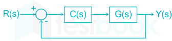
Consider the following closed-loop control system

Where G(s)=1s(s+1)G\left( s \right)=\frac{1}{s\left( s+1 \right)} and C(s)=Ks+1s+3C\left( s \right)=K\frac{s+1}{s+3}. If the steady-state error for a unit ramp input is 0.1, then the value of K is

Attempt this paper under real exam conditions

Timed interface, section switching, instant scoring, and question-by-question analytics — free.

Start Timed Attempt