Official Paper

GATE EC 2016 Official Paper: Shift 2 (Previous Year Paper)

65 questions · 180 minutes · with answers · free

General Aptitude (10 questions)

1

Based on the given statements, select the appropriate option with respect to grammar and usage.

Statements

(i) The height of Mr. X is 6 feet.

(ii) The height of Mr. Y is 5 feet.

  1. ((a))

    Mr. X is longer than Mr. Y.

  2. ((b))

    Mr. X is more elongated than Mr. Y.

  3. ((c))

    Mr. X is taller than Mr. Y.

  4. ((d))

    Mr. X is lengthier than Mr. Y.

Show Answer
Answer: ((c))

Mr. X is taller than Mr. Y.

Since the heights of two people are being compared, the correct adjective in the comparative degree to be used is “taller”.
2

The students ___________ the teacher on teachers’ day for twenty years of dedicated teaching.

  1. ((a))

    facilitated

  2. ((b))

    felicitated

  3. ((c))

    fantasized

  4. ((d))

    fecilitated

Show Answer
Answer: ((b))

felicitated

Let us look at the meanings of the words:

Facilitated: Helps improve something

Felicitated: Congratulate

Fantasize: Dream about something

The other option is not a word. Thus, the correct word to be used in the blank is ‘felicitated’ that will give the meaning of the teacher being congratulated.

3

After India’s cricket world cup victory in 1985, Shrotria who was playing both tennis and cricket till then, decided to concentrate only on cricket. And the rest is history.

What does the underlined phrase mean in this context?

  1. ((a))

    history will rest in peace

  2. ((b))

    rest is recorded in history books

  3. ((c))

    rest is well known

  4. ((d))

    rest is archaic

Show Answer
Answer: ((c))

rest is well known

The phrase ‘rest is history’ means something that has happened in the past and has become very famous. Thus ‘the rest is well known’ is the correct answer.

4

Given (9;inches)12=(0.25;yards)12{\left( {9{\rm{;inches}}} \right)^{\frac{1}{2}}} = {\left( {0.25{\rm{;yards}}} \right)^{\frac{1}{2}}}.  Which one of the following statements is TRUE?

  1. ((a))

    3 inches = 0.5 yards

  2. ((b))

    9 inches = 1.5 yards

  3. ((c))

    9 inches = 0.25 yards

  4. ((d))

    81 inches = 0.0625 yards

Show Answer
Answer: ((c))

9 inches = 0.25 yards

(9;inches)12=(0.25;yards)12{\left( {9{\rm{;inches}}} \right)^{\frac{1}{2}}} = {\left( {0.25{\rm{;yards}}} \right)^{\frac{1}{2}}}

Taking roots we have

3Inches=0.5Yards3\sqrt {Inches} = 0.5\sqrt {Yards}

inchesyards=0.53\frac{{\sqrt {inches} }}{{\sqrt {yards} }} = \frac{{0.5}}{3}

squaring both sides and cross multiplying we have 

9 inches = 0.25 yards

Method 2:

simply squaring both sides of the equation given in the question

we have 

9 inches = .25 yards

5

S, M, E and F are working in shifts in a team to finish a project. M works with twice the efficiency of others but for half as many days as E worked. S and M have 6 hour shifts in a day, whereas E and F have 12 hours shifts. What is the ratio of contribution of M to contribution of E in the project?

  1. ((a))

    1:1

  2. ((b))

    1:2

  3. ((c))

    1:4

  4. ((d))

    2:1

Show Answer
Answer: ((b))

1:2

Given:

M works with twice the efficiency of others but for half as many days as E worked

S and M have 6 hour shifts in a day, whereas E and F have 12 hours shifts

Calculation:

Let the efficiency of E be x then the efficiency of M is 2x.

Let M work for y day. Since E works for twice as long, E must work for 2y days.

Thus, amount of work done by M = 2x × y × 6

 and the amount of work done by E = x × 2y × 12

The ratio of work done by M to E is

⇒  ME=2x × y ×6x × 2y ×12=1:2\frac{{\rm{M}}}{{\rm{E}}} = \frac{{ {\rm{2x}} \ × \ {\rm{y} \ \times 6}}}{{{\rm{x}} \ × \ 2{\rm{y} \ \times 12}}} = 1:2.

∴ The contribution of M and E in the project is 1 : 2.

6

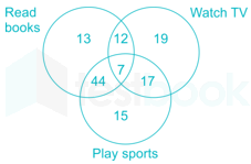
The Venn diagram shows the preference of the student population for leisure activities.

From the data given, the number of students who like to read books or play sports is ____.

  1. ((a))

    44

  2. ((b))

    51

  3. ((c))

    79

  4. ((d))

    108

Show Answer
Answer: ((d))

108

According to the given Venn diagram number of students who like to read books are.

13 + 12 + 44 + 7 = 76

Number of students who like to play sports are,

44 + 7 + 15 + 17 = 83

But the number of students who like both to read books and play sports are,

44 + 7 = 51

Hence the number of students who like to read books or play sports are,

76 + 83 – 51 = 108.

Here formula used is:

(No. of students Read books ⋃ no. of students play sports) ⋂ No of students read books 2 play sports.

7

Social science disciplines were in existence in an amorphous form until the colonial period when they were institutionalized. In varying degrees, they were intended to further the colonial interest. In the time of globalization and the economic rise of postcolonial countries like India, conventional ways of knowledge production have become obsolete.

Which of the following can be logically inferred from the above statements?

  1. Social science disciplines have become obsolete.
  2. Social science disciplines had a pre- colonial origin.
  3. Social science disciplines always promote colonialism
  4. Social science must maintain disciplinary boundaries.
  1. ((a))

    (ii) only

  2. ((b))

    (i) and (iii) only

  3. ((c))

    (ii) and (iv) only

  4. ((d))

    (iii) and (iv) only

Show Answer
Answer: ((a))

(ii) only

The passage does not state the boundaries of discipline for social sciences. Neither can this be inferred. Again, the passage only states that the social sciences were institutionalized because of colonial motives. This is not the same as promoting colonialism. Thus this cannot be inferred either. The knowledge production methods have become obsolete and not the discipline. Thus, point (i) is eliminated.

The passage states that social sciences discipline were in an amorphous form till the colonial period. This means that it existed before the colonial age. Thus point (ii) can be inferred.

8

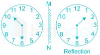
Two and a quarter hours back, when seen in a mirror, the reflection of a wall clock without number markings seemed to show 1:30. What is the actual current time shown by the clock?

  1. ((a))

    8:15

  2. ((b))

    11:15

  3. ((c))

    12:15

  4. ((d))

    12:45

Show Answer
Answer: ((d))

12:45

When reflection of a wall clock without number markings seemed to show 1:30 in a mirror, the actual time was 10:30 as shown in figure.

This was a time two and a quarter hours back.

Hence the actual current time is 10:30 + 2:15 = 12:45

9

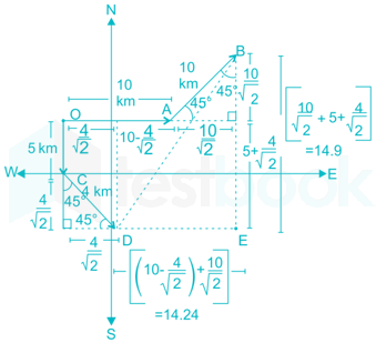
M and N start from the same location. M travels 10 km East and then 10 km North-East. N travels 5 km South and then 4 km South-East. What is the shortest distance (in km) between M and N at the end of their travel?

  1. ((a))

    18.60

  2. ((b))

    22.50

  3. ((c))

    20.61

  4. ((d))

    25.00

Show Answer
Answer: ((c))

20.61

Let both M;and;N{\rm{M;and;N}} start from origin. The position vector of M will be

PM=10i^+10cos45i^+10cos45j^=(10+102)i^+102j^{{\rm{\vec P}}_{\rm{M}}} = 10{\rm{\hat i}} + 10\cos {45^ \circ }{\rm{\hat i}} + 10\cos {45^ \circ }{\rm{\hat j}} = \left( {10 + \frac{{10}}{{\sqrt 2 }}} \right){\rm{\hat i}} + \frac{{10}}{{\sqrt 2 }}{\rm{\hat j}} 

Similarly, position vector of N will be,

PN=4cos45i^5j^4sin45j^=42i^(5+42)j^{{\rm{\vec P}}_{\rm{N}}} = 4\cos {45^ \circ }{\rm{\hat i}} - 5{\rm{\hat j}} - 4\sin {45^ \circ }{\rm{\hat j}} = \frac{4}{{\sqrt 2 }}{\rm{\hat i}} - \left( {5 + \frac{4}{{\sqrt 2 }}} \right){\rm{\hat j}} 

Displacement vector between M and N, \({{\rm{\vec P}}{{\rm{NM}}}} = {{\rm{\vec P}}{\rm{M}}} - {{\rm{\vec P}}_{\rm{N}}}\)

PNM=(10+10242)i^+(102+5+42)j^\Rightarrow {{\rm{\vec P}}_{{\rm{NM}}}} = \left( {10 + \frac{{10}}{{\sqrt 2 }} - \frac{4}{{\sqrt 2 }}} \right){\rm{\hat i}} + \left( {\frac{{10}}{{\sqrt 2 }} + 5 + \frac{4}{{\sqrt 2 }}} \right){\rm{\hat j}} 

Distance between them, PNM=(10+10242)2+(102+5+42)2\left| {{{{\rm{\vec P}}}_{{\rm{NM}}}}} \right| = \sqrt {{{\left( {10 + \frac{{10}}{{\sqrt 2 }} - \frac{4}{{\sqrt 2 }}} \right)}^2} + {{\left( {\frac{{10}}{{\sqrt 2 }} + 5 + \frac{4}{{\sqrt 2 }}} \right)}^2}}

PNM=20.612;m\Rightarrow \left| {{{{\rm{\vec P}}}_{{\rm{NM}}}}} \right| = 20.612{\rm{;m}}

10

A wire of length 340 mm is to be cut into two parts. One of the parts is to be made into a square and the other into a rectangle where sides are in the ratio of 1:2. What is the length of the side of the square (in mm) such that the combined area of the square and the rectangle is a MINIMUM?

  1. ((a))

    30

  2. ((b))

    40

  3. ((c))

    120

  4. ((d))

    180

Show Answer
Answer: ((b))

40

Let the side of square formed be y. And the length and breadths of the rectangle formed by 2x and x as they are in the ratio 2:1. Then, Perimeter of square P(S)=4y{\rm{P}}\left( {\rm{S}} \right) = 4{\rm{y}} and perimeter of  rectangle P(R)=6x{\rm{P}}\left( {\rm{R}} \right) = 6{\rm{x}}. Since this all length is cut form the 340 mm wire, we have P(S)+P(R)=340{\rm{P}}\left( {\rm{S}} \right) + {\rm{P}}\left( {\rm{R}} \right) = 340

4y+6x=340 y=8532x\begin{array}{l} \Rightarrow 4{\rm{y}} + 6{\rm{x}} = 340\ \Rightarrow {\rm{y}} = 85 - \frac{3}{2}{\rm{x}} \end{array} 

Now the combined are of square and rectangle, A=y2+2x2{\rm{A}} = {{\rm{y}}^2} + 2{{\rm{x}}^2}

Substituting the value of y we have,

A=(8532x;)2+2x2 A=7225+94x2255x+2x2; A=17x21020x+289002;\begin{array}{l} {\rm{A}} = {\left( {85 - \frac{3}{2}{\rm{x;}}} \right)^2} + 2{{\rm{x}}^2}\ \Rightarrow {\rm{A}} = 7225 + \frac{9}{4}{{\rm{x}}^2} - 255{\rm{x}} + 2{{\rm{x}}^2}{\rm{;}}\ \Rightarrow {\rm{A}} = \frac{{17{{\rm{x}}^2} - 1020{\rm{x}} + 28900}}{2}{\rm{;}} \end{array} 

Form minimum area,  dAdx=0\frac{{{\rm{dA}}}}{{{\rm{dx}}}} = 0

dAdx=34x1020=0 x=102034=30\begin{array}{l} \Rightarrow \frac{{{\rm{dA}}}}{{{\rm{dx}}}} = 34{\rm{x}} - 1020 = 0\ \Rightarrow {\rm{x}} = \frac{{1020}}{{34}} = 30 \end{array}

Now, length of the side of the square

y=8532×30=8545=40mm{\rm{y}} = 85 - \frac{3}{2} \times 30 = 85 - 45 = 40{\rm{mm}}

Electronics and Communication Engineering (55 questions)

11

The value of x for which the matrix \({\rm{A}} = \left[ {\begin{array}{*{20}{c}} 3&2&14\ 9&7&{13}\ { - 6}&{ - 4}&{ - 9 + {\rm{x}}} \end{array}} \right]\) has zero as an eigenvalue is ________

12

Consider the complex valued function f(z)=2z3+bz3\rm f(z) = 2z^3 + b |z|^3 where z\rm z is a complex variable.

The value of b\rm b for which the function f(z){\rm{f}}\left( {\rm{z}} \right) is analytic is ________

13

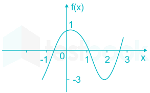
As x\rm x varies from 1 to +3\rm −1\ to \ +3, which one of the following describes the behaviour of the function f(x)=x33x2+1\rm f(x) = x^3 – 3x^2 + 1?

  1. ((a))

    f(x)\rm f(x) increases monotonically.

  2. ((b))

    f(x)\rm f(x) increases, then decreases and increases again.

  3. ((c))

    f(x)\rm f(x) decreases, then increases and decreases again.

  4. ((d))

    f(x)\rm f(x) increases and then decreases.

Show Answer
Answer: ((b))

f(x)\rm f(x) increases, then decreases and increases again.

Concept:

Whenever we have to analyse the graph for a given function generally substitute consecutive numbers and define. Here the range is already specified simply we can substitute those values in a given function and then we can draw a graph based on results

Calculation:

Given f(x) = x3 – 3x2 + 1, x varies from -1 to 3

x = -1, f(X) = (-1)3 – 3(-1)2 + 1 = -1 -3 + 1 = -3

x = 0, f(x) = (0)3 – 3(0)2 + 1 = 0 – 0 + 1 = 1

x = 1, f(x) = (1)3 – 3(1)2 + 1 = 1 – 3 + 1 = -1

x = 2, f(x) = (2)3 – 3(2)2 + 1 = 8 – 12 + 1 = -3

x = 3, f(x) = (3)3 – 3(3)2 + 1 = 27 – 27 +1 = 1

X-10123
f(x)-31-1-31


Graph Result:

From the calculation graph is first increases, then decreases and increases again

Alternate Method:

Given f(x) = x3 – 3x2 + 1

Let us first find the stationary points by making f’(x) = 0 & then we will decide for maxima & minima by the sign of f”(x) at that point

f'(x) = 3x2 – 6x

3x2 – 6x = 0

3x (x - 2) = 0

x = 0, 2

x = 0 & x = 2 are stationary points.

f"(x) = 6 × -6

f”(0) = -6 < 0 Hence, maxima

f”(2) = 6 > 0 Hence, minima

f(-1) = 3

f(0) = 1

f(2) = -3

f(3) 1

f(x) increases, then decreases & increases again.

So, option B is true.

14

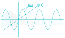
How many distinct values of x\rm x satisfy the equation sin(x)=x/2\rm sin(x) = x/2, where x\rm x is in radians?

  1. ((a))

    1

  2. ((b))

    2

  3. ((c))

    3

  4. ((d))

    4 or more

Show Answer
Answer: ((c))

3

Given sinx=x2{\rm{sinx}} = \frac{{\rm{x}}}{2}

let f(x)=sinx\rm f(x) = sin x and g(x)=x/2\rm g(x) = x / 2

∴ The given function has 3 distinct roots

15

Consider the time-varying vector I=x^;15cos(wt)+y^;5{\bf{I}} = {\rm{\hat x;}}15\cos \left( {{\rm{wt}}} \right) + {\rm{\hat y;}}5 sin(𝜔𝑡) in Cartesian coordinates, where 𝜔 > 0 is a constant. When the vector magnitude |𝐈| is at its minimum value, the angle 𝜃 that 𝐈 makes with the 𝑥 axis (in degrees, such that 0 ≤ 𝜃 ≤ 180) is ________

16

In the circuit shown below, VS is a constant voltage source and IL is a constant current load.

The value of IL\rm I_L that maximizes the power absorbed by the constant current load is

  1. ((a))

    Vs4R\frac{{{{\rm{V}}_{\rm{s}}}}}{{4{\rm{R}}}}

  2. ((b))

    Vs2R\frac{{{{\rm{V}}_{\rm{s}}}}}{{2{\rm{R}}}}

  3. ((c))

    VsR\frac{{{{\rm{V}}_{\rm{s}}}}}{{\rm{R}}}

  4. ((d))

    \rm\infty

Show Answer
Answer: ((b))

Vs2R\frac{{{{\rm{V}}_{\rm{s}}}}}{{2{\rm{R}}}}

For the given circuit,

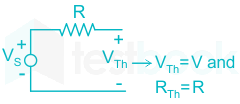
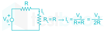
The equivalent Thevenin circuit is given as

The maximum power transfer for the resistive circuit is possible when

RL = RTh = R

Front the above figure the load current can be derived as

\( {{\rm{I}}{\rm{L}}} = \frac{{{{\rm{V}}{\rm{s}}}}}{{{\rm{R}} + {\rm{R}}}}\)

IL = Vs/2R

Hence option (2) is correct

The power across Load RL = R is given by

Pmax=(Vs2R)2.RP_{max} = {(\frac{V_s}{2R})}^2.R

Pmax=Vs24RP_{max} = \frac{{V_s}^2}{4R}

Load variableThe load impedance for maximum power transfer
RL and XL are variableRL = RS XL = -XS ZL = ZS*
RL only varied and XL = ConstantRL =√(RS2 + (XL + XS)2)
RL only varied and XL = 0RL =√(RS2 + XS2)
17

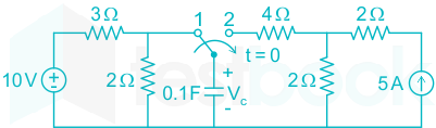
The switch has been in position 1 for a long time and abruptly changes to position 2 at t = 0.

.

If time t\rm t is in seconds, the capacitor voltage VC\rm V_C (in volts) for t>0\rm t > 0 is given by

  1. ((a))

    4(1exp(t/0.5))\rm 4(1 − exp(−t/0.5))

  2. ((b))

    106 exp(t/0.5)\rm 10 − 6\ exp(−t/0.5)

  3. ((c))

    4(1exp(t/0.6))\rm 4(1 − exp(−t/0.6))

  4. ((d))

    106exp(t/0.6)\rm 10 − 6 exp(−t/0.6)

Show Answer
Answer: ((d))

106exp(t/0.6)\rm 10 − 6 exp(−t/0.6)

Concept:

For t > 0, capacitor voltage Vc(t) is given as,

VC(t)=[VC(0+)VC()]et/τ+VC(){V_C}\left( t \right) = \left[ {{V_C}\left( {{0^ + }} \right) - {V_C}\left( \infty \right)} \right]{e^{ - t/\tau }} + {V_C}\left( \infty \right)        ---(1)

Where,

VC(0+): Voltage across capacitor at t = 0+

VC(0): Voltage across capacitor at steady state

τ :Time constant = Req Ceq

Calculation:

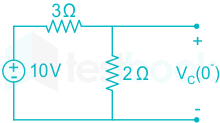
At  t = 0-, switch is at position – 1

Capacitor behaves open circuit at t = 0- (steady state)

VC(0)=2×10³+2{V_C}\left( {{0^ - }} \right) = \frac{{2 \times 10}}{{3 + 2}} 

VC(0-) = 4 V

We know that, capacitor opposes sudden change in voltage

So,

VC(0-) = VC(0+) = 4V

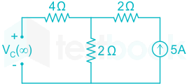
Now, at t = ∞, the switch is at position – 2

VC(∞) = 5 × 2 = 10 V

Calculation of time constant:

Draw the Circuit at t > 0 and open circuit the current source,

Req = 4 + 2 = 6Ω

So,

τ = Req⋅ Ceq = 6 Ω × .1F = 0.6 sec

Now from equation (1), we get:

VC(t)=VC()+[VC(0+)VL()]et/τ{V_C}\left( t \right) = {V_C}\left( \infty \right) + \left[ {{V_C}\left( {{0^ + }} \right) - {V_L}\left( \infty \right)} \right]{e^{ - t/\tau }} 

VC(t)=[106et0.6]V{V_C}\left( t \right) = \left[ {10 - 6{e^{ - \frac{t}{{0.6}}}}} \right]V

18

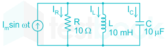
The figure shows an RLC circuit with a sinusoidal current source:

At resonance, the ratio |𝐈𝐋|/|𝐈𝐑|, i.e., the ratio of the magnitudes of the inductor current phasor and the resistor current phasor, is ________

19

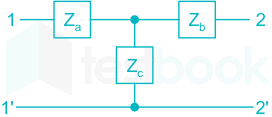
The z-parameter matrix for the two-port network shown is

\(\left[ {\begin{array}{*{20}{c}} {2{\rm{jω }}}&{{\rm{jω }}}\ {{\rm{jω }}}&{3 + 2{\rm{jω }}} \end{array}} \right]\)

where the entries are in Ω. Suppose Zb(jω) = Rb + jω.

Then the value of Rb (in Ω) equals ________.

20

The energy of the signal x(t)=sin(4πt)4πtx(t) = \frac{{{\rm{sin}}\left( {4{\rm{\pi t}}} \right)}}{{4{\rm{\pi t}}}}  is______

21

The Ebers-Moll model of a BJT is valid

  1. ((a))

    only in active mode

  2. ((b))

    only in active and saturation modes

  3. ((c))

    only in active and cut-off modes

  4. ((d))

    in active, saturation and cut-off modes

Show Answer
Answer: ((d))

in active, saturation and cut-off modes

Ebers-Moll model is valid for all of the active, saturation and cutoff regions.

22

A long-channel NMOS transistor is biased in the linear region with VDS=50 mV\rm V_{DS}=50\ mV and is used as a resistance. Which one of the following statements is NOT correct?

  1. ((a))

    If the device width W is increased, the resistance decreases.

  2. ((b))

    If the threshold voltage is reduced, the resistance decreases.

  3. ((c))

    If the device length L is increased, the resistance increases.

  4. ((d))

    If VGS is increased, the resistance increases.

Show Answer
Answer: ((d))

If VGS is increased, the resistance increases.

Concept:

For VDS < VGS – VT, n-channel enhancement type MOSFET will operate in triode/linear region:

ID=WμnCox2L[2(VGSVT)VDSVDS2]{I_D} = \frac{{{\rm{W\mu_n }}{C_{ox}}}}{{2L}}\left[ {2\left( {{V_{GS}} - {V_T}} \right){V_{DS}} - V_{DS}^2} \right]

For VDS ≥ VGS – VT, the MOSFET will be in saturation with current given by:

ID=WμnCox2L[(VGSVT)2]{I_D} = \frac{{{\rm{W\mu_n }}{C_{ox}}}}{{2L}}\left[ {{{\left( {{V_{GS}} - {V_T}} \right)}^2}} \right]

Application:

The current in an NMOS in the linear region, therefore:

ID=WμnCox2L[2(VGSVT)VDSVDS2]{I_D} = \frac{{{\rm{W\mu_n }}{C_{ox}}}}{{2L}}\left[ {2\left( {{V_{GS}} - {V_T}} \right){V_{DS}} - V_{DS}^2} \right]

The transistor operates in the linear region for small values of VDS

IDWμnCoxL[(VGSVT)VDS]{I_D} \approx \frac{{{\rm{W\mu_n }}{C_{ox}}}}{{L}}\left[ {\left( {{V_{GS}} - {V_T}} \right){V_{DS}}} \right]

Rd=VDSIDSR_d=\frac{V_{DS}}{I_{DS}}

Rd=1WμnCoxL[(VGSVT)VDS]R_d=\frac{1}{\frac{{{\rm{W\mu_n }}{C_{ox}}}}{{L}}\left[ {\left( {{V_{GS}} - {V_T}} \right){V_{DS}}} \right]}

Observations:

  • As W increases, the resistance decreases.
  • As VT decreases, the resistance decreases.
  • As L increases, the resistance increases.
  • However, as VGS increases, the resistance decreases. So, Option D is the required incorrect statement
23

Assume that the diode in the figure has Von = 0.7 V, but is otherwise ideal.

The magnitude of the current i2 (in mA) is equal to ________

24

Resistor R1 in the circuit below has been adjusted such that I1 = 1 mA. The bipolar transistors Q1 and Q2 are perfectly matched and have very high current gain, so their base currents are negligible. The supply voltage VCC is 6 V. The thermal voltage kT/q is 26 mV.

The value of R2 (in Ω) for which I2 = 100 μA is ________

25

Which one of the following statements is correct about an ac-coupled common-emitter amplifier operating in the mid-band region?

  1. ((a))

    The device parasitic capacitances behave like open circuits, whereas coupling and bypass capacitances behave like short circuits.

  2. ((b))

    The device parasitic capacitances, coupling capacitances and bypass capacitances behave like open circuits.

  3. ((c))

    The device parasitic capacitances, coupling capacitances and bypass capacitances behave like short circuits.

  4. ((d))

    The device parasitic capacitances behave like short circuits, whereas coupling and bypass capacitances behave like open circuits.

Show Answer
Answer: ((a))

The device parasitic capacitances behave like open circuits, whereas coupling and bypass capacitances behave like short circuits.

We know that:

XC=1ωC=12πfC\left| {{X_C}} \right| = \frac{1}{{\omega C}} = \frac{1}{{2\pi fC}} 

  • The parasitic capacitances are in PF (10-12 f) So, |XC| becomes too large (≈ ∞) for the mid freq. band so parasitic capacitance act line open circuit.
  • The bypass and coupling capacitances are in μf (10-6f) so, Xc becomes very small (≈ 0) for the mid-frequency band so, they behave as a short circuit.

Note:

CapacitorsMid Freq.Low Freq.High Freq.
1. Large-cap. (μf)Short circuitEffect is consideredShort circuit
2. Small-cap (PF)Open circuitOpen circuitEffect is considered
26

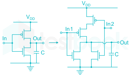
Transistor geometries in a CMOS inverter have been adjusted to meet the requirement for worst-case charge and discharge times for driving a load capacitor C. This design is to be converted to that of a NOR circuit in the same technology, so that its worst-case charge and discharge times while driving the same capacitor are similar. The channel lengths of all transistors are to be kept unchanged. Which one of the following statements is correct?

  1. ((a))

    Widths of PMOS transistors should be doubled, while widths of NMOS transistors should be halved.

  2. ((b))

    Widths of PMOS transistors should be doubled, while widths of NMOS transistors should not be changed.

  3. ((c))

    Widths of PMOS transistors should be halved, while widths of NMOS transistors should not be changed.

  4. ((d))

    Widths of PMOS transistors should be unchanged, while widths of NMOS transistors should be halved.

Show Answer
Answer: ((b))

Widths of PMOS transistors should be doubled, while widths of NMOS transistors should not be changed.

Generally the area of PMOS is double to NMOS to maintain equal rise time and fall time.

Because mobility of electron is double that of mobility of hole. The (WL)\left( {\frac{{\rm{W}}}{{\rm{L}}}} \right) of PMOS can be calculated by dividing its resistance with 2R whereas the (WL)\left( {\frac{{\rm{W}}}{{\rm{L}}}} \right) of NMOS can be calculated by dividing its resistance with R.

The (WL)\left( {\frac{{\rm{W}}}{{\rm{L}}}} \right) of first circuit:

\({\left( {\frac{{\rm{W}}}{{\rm{L}}}} \right){\rm{p}}} = \frac{{2{\rm{R}}}}{{\rm{R}}} = 2\) and \({\left( {\frac{{\rm{W}}}{{\rm{L}}}} \right){\rm{p}}} = \frac{{\rm{R}}}{{\rm{R}}} = 1\)

The (WL)\left( {\frac{{\rm{W}}}{{\rm{L}}}} \right) of second circuit:

\({\left( {\frac{{\rm{W}}}{{\rm{L}}}} \right){\rm{p}}} = \frac{{2{\rm{R}}}}{{{\rm{R}}/2}} = 4\) and \({\left( {\frac{{\rm{W}}}{{\rm{L}}}} \right){\rm{n}}} = \frac{{\rm{R}}}{{\rm{R}}} = 1\)

So the width of PMOS is doubled and width of NMOS remains same.

27

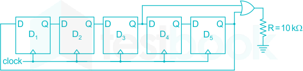
Assume that all the digital gates in the circuit shown in the figure are ideal, the resistor R = 10 kΩ, and the supply voltage is 5 V. The D flip-flops D1, D2, D3, D4, and D5 are initialized with logic values 0, 1, 0, 1, and 0 respectively. The clock has a 30% duty cycle.

The average power dissipated (in mW) in the resistor R is ________

28

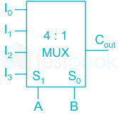
A 4:1 multiplexer is to be used for generating the output carry of a full adder. A and B are the bits to be added while Cin is the input carry and Cout is the output carry. A and B  are to be used as the select bits with A being the more significant select bit.

  1. ((a))

    I0 = 0, I1 = Cin, I2 = Cin and I3 = 1

  2. ((b))

    I0 = 1, I1 = Cin, I2 = Cin and I3 = 1

  3. ((c))

    I0 = Cin, I1 = 0, I2 = 1 and I3 = Cin

  4. ((d))

    I0 = 1, I1 = Cin, I2 = 1 and I3 = Cin

Show Answer
Answer: ((a))

I0 = 0, I1 = Cin, I2 = Cin and I3 = 1

Concept:

The functional table is mentioned below:

S0S1Y
001
011
101
111


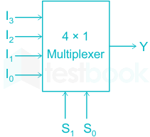
The general output equation is:

Y=S1S0;I0+S1S0I1+S1S0;I2+S1S0I3Y = \overline {{S_1}} \overline {{S_0}} ;{I_0} + \overline {{S_1}} {S_0}{I_1} + {S_1}\overline {{S_0}} ;{I_2} + {S_1}{S_0}{I_3}

The truth table for a full adder is as shown:

ABCiCoutS
00000
00101
01001
01110
10001
10110
11010
11111


The expression for the sum bit and the output carry will be:

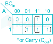
Cout = ∑ m (3, 5, 6, 7) and

S = ∑ m (1, 2, 4, 7)

Another equation for Cout is:

Cout=(Aˉ;B+A;Bˉ)Ci+ABC_{out}=\left( {\bar A;B + A;\bar B} \right){C_i} + AB

Calculation:

Given S1 = A and S0 = B. The output expression becomes:

Y=;Aˉ;Bˉ;Ci+Aˉ;B;Ci+ABˉ;Ci+ABCY = ;\bar A;\bar B;{C_i} + \bar A;B;{C_i} + A\bar B;{C_i} + ABC   ---(iii)

The equation for Cout is:

Cout=(Aˉ;B+A;Bˉ)Ci+ABC_{out}=\left( {\bar A;B + A;\bar B} \right){C_i} + AB

Cout=Aˉ;B;Ci+ABˉ;Ci+ABC_{out}=\bar A;B;{C_i} + A\bar B;{C_i} + AB  ---(iv)

Comparing equations (iii) and (iv), we get:

I0 = 0, I1 = Cin, I2 = Cin, I3 = 1

29

The response of the system G(s)=s2(s+1)(s+3){\rm{G}}\left( {\rm{s}} \right) = \frac{{{\rm{s}} - 2}}{{\left( {{\rm{s}} + 1} \right)\left( {{\rm{s}} + 3} \right)}} to the unit step input u(t)\rm u(t) is y(t)\rm y(t).

The value of dydt\frac{{{\rm{dy}}}}{{{\rm{dt}}}} at t=0+\rm t = 0^+ is _________

30

The number and direction of encirclements around the point 1+j0\rm −1 + j0 in the complex plane by the Nyquist plot of G(s)=1s4+2s{\rm{G}}\left( {\rm{s}} \right) = \frac{{1 - {\rm{s}}}}{{4 + 2{\rm{s}}}} is

  1. ((a))

    zero.

  2. ((b))

    one, anti-clockwise.

  3. ((c))

    one, clockwise.

  4. ((d))

    two, clockwise.

Show Answer
Answer: ((a))

zero.

Concept:

The Nyquist plot is equal to the polar plot & mirror Image of the polar plot with respect to the real axis, with opposite direction + semicircle of the infinite radius in a clockwise direction as many as the type of system.

Calculation:

Given:

G(s)=1s4+2sG\left( s \right) = \frac{{1 - s}}{{4 + 2s}} 

G(jω)=1jω4+2jωG\left( {j\omega } \right) = \frac{{1 - j\omega }}{{4 + 2j\omega }} 

So,

G(jω)=1+ω216+4ω2\left| {G\left( {j\omega } \right)} \right| = \frac{{\sqrt {1 + {\omega ^2}} }}{{\sqrt {16 + 4{\omega ^2}} }} 

G(jω)=;tan1ωtan1ω2\angle G\left( {j\omega } \right) = ; - {\tan ^{ - 1}}\omega - {\tan ^{ - 1}}\frac{\omega }{2}

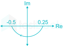
ω|G(jω)|∠G(jω)
0.25
-0.5-180°


Polar plot of Given G(s) is

Now,

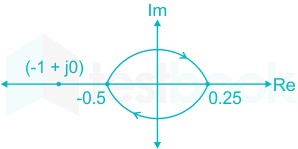
Nyquist plot of Given G(s) is:

Hence, the number of Encirclements of (-1 + j0) = 0

31

A discrete memoryless source has an alphabet {a1, a2, a3, a4}  with corresponding probabilities \(\left{ {\frac{1}{2},\frac{1}{4},\frac{1}{8},\frac{1}{8}} \right}\). The minimum required average codeword length in bits to represent this source for error-free reconstruction is ________

32

A speech signal is sampled at 8 kHz and encoded into PCM format using 8 bits/sample. The PCM data is transmitted through a baseband channel via 4-level PAM. The minimum bandwidth (in kHz) required for transmission is ________

33

A uniform and constant magnetic field  B ẑ. exists in the \({\rm{̂ z}}\) direction in vacuum. A particle of mass m  with a small charge q is introduced into this region with an initial velocity v = x̂vx + ẑvz. Given that B, m, q, vx, and vz are all non-zero, which one of the following describes the eventual trajectory of the particle?

  1. ((a))

    Helical motion in the ẑ direction.

  2. ((b))

    Circular motion in the xy-plane.

  3. ((c))

    Linear motion in the ẑ direction.

  4. ((d))

    Linear motion in the x̂ direction.

Show Answer
Answer: ((a))

Helical motion in the ẑ direction.

Concept:

When any non-zero charge enters in a magnetic field with some velocity at an angle other than 90 degrees, then charge follow helical trajectory.

Application:

B=Bz^0\vec B = B{\hat z_0}

V=vXx^+vZz^\vec V = {v_X}\hat x + {v_Z}\hat z

x-component of V\vec V is perpendicular to the magnetic field B\vec B.

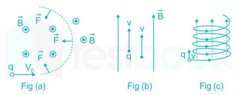
A charge moving perpendicular to the magnetic field will experience a radial force causing circular motion shown in figure (a).

z-component of V\vec V is parallel to the magnetic field B\vec B. A change moving parallel to the field generates no force shown in figure (b).

Motion with components perpendicular and parallel to the field causes the change to move in a helical path along +z direction as shown in figure (c).

34

Let the electric field vector of a plane electromagnetic wave propagating in a homogenous medium be expressed as E=x^Exe(ωtβz)\rm \vec E={\rm{\hat x}}E_xe^{−(\omega t-\beta z)} , where the propagation constant β\rm \beta is a function of the angular frequency ω\rm \omega. Assume that β(ω)\rm \beta(\omega) and Ex\rm E_x are known and are real. From the information available, which one of the following CANNOT be determined?

  1. ((a))

    The type of polarization of the wave.

  2. ((b))

    The group velocity of the wave.

  3. ((c))

    The phase velocity of the wave.

  4. ((d))

    The power flux through the z=0\rm z = 0 plane.

Show Answer
Answer: ((d))

The power flux through the z=0\rm z = 0 plane.

Let us analyze each option.

Option A: Because polarization is nothing but the orientation of the electric field vector. we can determine the polarization of the wave.

So option A is incorrect.

Option B:

The group velocity (vg) of the wave is given by:

vg=dωdβ{v_g} = \frac{{d\omega }}{{d\beta }} 

Since β(ω) is known, we can find dβdω\frac{{d\beta }}{{d\omega }} and hence the group velocity will be:

vg=1dβdω{v_g} = \frac{1}{{\frac{{d\beta }}{{d\omega }}}} 

So option B is incorrect.

Option C:

The phase velocity (vp) is defined as:

vP=ωβ{v_P} = \frac{\omega }{\beta } 

This can also be determined

So, option C is incorrect.

Option D:

The power flux through the z = 0 plane is:

P=12ε02ηP = \frac{1}{2}\frac{{\varepsilon _0^2}}{\eta } 

Since only E is given, we cannot determine the intrinsic impedance of the medium from the given data. Hence power flux through any plane cannot be determined.

Hence option D is Correct.

35

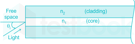
Light from free space is incident at an angle θ1to the normal of the facet of a step-index large core optical fibre. The core and cladding refractive indices are n1 = 1.5 and n2 = 1.4, respectively.

The maximum value of θ(in degrees) for which the incident light will be guided in the core of the fibre is ________.

36

The ordinary differential equation dydt=3x+2,with x(0);=;1\frac{{{\rm{dy}}}}{{{\rm{dt}}}} = - 3{\rm{x}} + {\rm{}}2,{\rm{with\ x}}\left( 0 \right){\rm{;}} = {\rm{;}}1

is to be solved using the forward Euler method. The largest time step that can be used to solve the equation without making the numerical solution unstable is ________.

37

Suppose C is the closed curve defined as the circle x2+y2=1\rm x^2 + y^2 = 1 with C\rm C oriented anti-clockwise. The value of (xy2dx+x2ydy)\rm ∮(xy^2 dx + x^2y dy) over the curve C\rm C equals ________

38

Two random variables X\rm X and Y\rm Y are distributed according to

\({\rm{f_{X,{{\rm{Y}}}}}{\left( {{\rm{x}},{\rm{y}}} \right)}} = \left{ {\begin{array}{*{20}{c}} {\left( {{\rm{x}} + {\rm{y}}} \right)}&{{\rm{0}} \le {\rm{x}} \le 1}&{0 \le {\rm{y}} \le 1}\ {0,}&{{\rm{otherwise}}.}&{\rm{;}} \end{array}} \right.\)

The probability (X+Y1)\rm (X+Y \le 1) is ________

39

The matrix \({\rm{A}} = \left[ {\begin{array}{*{20}{c}} {\rm{a}}&0&3&7\ 2&5&1&3\ 0&0&2&4\ 0&0&0&{\rm{b}} \end{array}} \right]\) has det(A)=100\rm det(A) = 100 and trace(A)=14\rm trace(A) = 14.

The value of ab\rm |a-b| is ________.

40

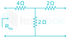
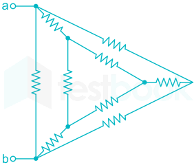
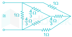
In the given circuit, each resistor has a value equal to 1 Ω.

What is the equivalent resistance across the terminals 𝑎 and 𝑏?

  1. ((a))

    1/6 Ω

  2. ((b))

    1/3 Ω

  3. ((c))

    9/20 Ω

  4. ((d))

    8/15 Ω

Show Answer
Answer: ((d))

8/15 Ω

Concept:

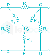
To convert Star from Delta, we follow the following procedure:

Branch resistance = product of connected resistance/sum of all resistances

For branch resistance, PS, Ra, and Rb are connected, so:

RA=Ra×RbRa+Rb+Rc{R_A} = \frac{{{R_a} \times {R_b}}}{{{R_a} + {R_b} + {R_c}}}

For branch resistance QS, Ra and Rc are connected, so:

RB=Ra×RcRa+Rb+Rc{R_B} = \frac{{{R_a} \times {R_c}}}{{{R_a} + {R_b} + {R_c}}}

For branch resistance, SR, Rb, and Rc are connected, so:

RC=Rc×RbRa+Rb+Rc{R_C} = \frac{{{{R_c} \times {R_b}}}}{{{R_a} + {R_b} + {R_c}}}

Calculation:

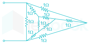
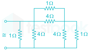
Covert Delta Network to star Network we get

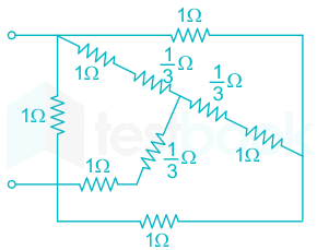
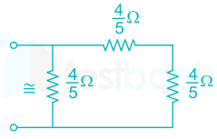
Covert star Network to delta Network we get

Req=45×8545+85=3225125 Ω{{\rm{R}}_{{\rm{eq}}}} = \frac{{\frac{4}{5} \times \frac{8}{5}}}{{\frac{4}{5} + \frac{8}{5}}} = \frac{{\frac{{32}}{{25}}}}{{\frac{{12}}{{5}}}} ~\Omega

Req = 32/60 = 8/15 Ω

41

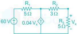
In the circuit shown in the figure, the magnitude of the current (in amperes) through R2 is ________.

42

A continuous-time filter with transfer function  H(s)=2s+6s2+6s+8;{\rm{H}}\left( {\rm{s}} \right) = \frac{{2{\rm{s}} + 6}}{{{{\rm{s}}^2} + 6{\rm{s}} + 8}}{\rm{;}}  is converted to a discretetime filter with transfer function G(z)=2z20.5032zz20.5032z+k{\rm{G}}\left( {\rm{z}} \right) = \frac{{2{{\rm{z}}^2} - 0.5032{\rm{z}}}}{{{{\rm{z}}^2} - 0.5032{\rm{z}} + {\rm{k}}}}  so that the impulse response of the continuous-time filter, sampled at 2 Hz\rm 2\ Hz, is identical at the sampling instants to the impulse response of the discrete time filter. The value of k\rm k is ________

43

The Discrete Fourier Transform (DFT) of the 4-point sequence

x[n]=x[0],x[1],x[2],x[3]=3,2,3,4\rm x[n] = {x[0], x[1], x[2], x[3]} = {3, 2, 3, 4} is

X[k]=X[0],X[1],X[2],X[3]=12,2j,0,2j\rm X[k] = {X[0], X[1], X[2], X[3]} = {12, 2j, 0, −2j}.

If X1[k]\rm X_1[k] is the DFT of the 12-point sequence x1[n]=3,0,0,2,0,0,3,0,0,4,0,0\rm x_1[n] = {3, 0, 0, 2, 0, 0, 3, 0, 0, 4, 0, 0}, the value of \(\left| {\frac{{{{\rm{X}}_1}\left[ 8 \right]}}{{{{\rm{X}}1{\left[ {11} \right]}}{\rm{;}}}}} \right|\) is ________

44

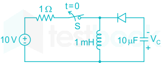
The switch S in the circuit shown has been closed for a long time.

It is opened at time t = 0 and remains open after that. Assume that the diode has zero reverse current and zero forward voltage drop.

The steady-state magnitude of the capacitor voltage Vc (in Volts) is ________.

45

A voltage VG\rm V_G is applied across a MOS capacitor with metal gate and p-type silicon substrate at T=300 K\rm T=300 \ K. The inversion carrier density (in number of carriers per unit area) for VG=0.8 V\rm V_G = 0.8 \ V is 2×1011cm2\rm 2 × 10^{11} cm^{−2}. For VG=1.3 V\rm V_G = 1.3 \ V, the inversion carrier density is 4×1011cm2\rm 4 × 10^{11} cm^{−2}. What is the value of the inversion carrier density for VG=1.8 V\rm V_G = 1.8 \ V?

  1. ((a))

    4.5×1011cm2\rm 4.5 × 10^{11} cm^{−2}

  2. ((b))

    6×1011cm2\rm 6 × 10^{11} cm^{−2}

  3. ((c))

    7.2×1011cm2\rm 7.2 × 10^{11} cm^{−2}

  4. ((d))

    8.4×1011cm2\rm 8.4 × 10^{11} cm^{−2}

Show Answer
Answer: ((b))

6×1011cm2\rm 6 × 10^{11} cm^{−2}

Concept:

In MOS capacitor charges Accumulated near the Interface is known as the Inversion carrier density (Q).

It is given as,

Q ∝ (VG - VT)

Where,

Q – Inversion carrier density (cm-2)

VG – Applied Gate voltage

VT – Thermal voltage.

Calculation:

Given:

VG1=.8;V{V_{{G_1}}} = .8;V, Q1 = 2 × 10¹¹,

VG2=1.3;V{V_{{G_2}}} = 1.3;V, Q2 = 4 × 10¹¹

VG3=1.8;V{V_{{G_3}}} = 1.8;V, Q3 = ?

We know that,

Q ∝ (VG - VT)

So,

VG1VTVG2VT=Q1Q2.8VT1.3VT=2×10114×1011\frac{{{V_{{G_1}}} - {V_T}}}{{{V_{{G_2}}} - {V_T}}} = \frac{{{Q_1}}}{{{Q_2}}} \Rightarrow \frac{{.8 - {V_T}}}{{1.3 - {V_T}}} = \frac{{2 \times {{10}^{11}}}}{{4 \times {{10}^{11}}}} 

On solving, we’ll get

VT = 0.3 V

Now,

VG2VTVG3VT=Q2Q3\frac{{{V_{{G_2}}} - {V_T}}}{{{V_{{G_3}}} - {V_T}}} = \frac{{{Q_2}}}{{{Q_3}}} 

1.30.31.80.3=4×10¹¹Q3\frac{{1.3 - 0.3}}{{1.8 - 0.3}} = \frac{{4 \times {{10}^{11}}}}{{{Q_3}}} 

Hence,

Inversion carrier density with VG = 1.8 V is

Q3 = 6 × 10¹¹ /cm2

46

Consider avalanche breakdown in a silicon p+n\rm p^+n junction. The n-region is uniformly doped with a donor density ND\rm N_D. Assume that breakdown occurs when the magnitude of the electric field at any point in the device becomes equal to the critical field Ecrit\rm E_{crit}. Assume Ecrit\rm E_{crit} to be independent of ND\rm N_D. If the built-in voltage of the p+n\rm p^+n junction is much smaller than the breakdown voltage, VBR\rm V_{BR}, the relationship between VBR\rm V_{BR} and ND\rm N_D is given by

  1. ((a))

    \({{\rm{V}}{{\rm{BR}}}} \times \sqrt {{{\rm{N}}{\rm{D}}}}\) constant

  2. ((b))

    \({{\rm{N}}{\rm{D}}} \times \sqrt {{{\rm{V}}{{\rm{BR}}}}}\) constant

  3. ((c))

    \({{\rm{N}}{\rm{D}}} \times {{\rm{V}}{{\rm{BR}}}}\) constant

  4. ((d))

    \({{\rm{N}}{\rm{D}}}/{{\rm{V}}{{\rm{BR}}}}\) constant

Show Answer
Answer: ((c))

\({{\rm{N}}{\rm{D}}} \times {{\rm{V}}{{\rm{BR}}}}\) constant

Analysis:

In any type of PN junction;

Ecritical =Vbi+VRBW/2= \frac{{{V_{bi}} + {V_{RB}}}}{{W/2}} 

Ecritical =2[Vbi+VRB]W = \frac{{2\left[ {{V_{bi}} + {V_{RB}}} \right]}}{W}        ---(1)

Where,

Vbi: Built-in potential.

VRB: Reverse bias voltage.

W=2εq(1NA+1ND)(Vbi+VRB)W = \sqrt {\frac{{2\varepsilon }}{q}\left( {\frac{1}{{{N_A}}} + \frac{1}{{{N_D}}}} \right)\left( {{V_{bi}} + {V_{RB}}} \right)}          ---(2)

P+N junction is given so

NAND;;So,;;1NA1ND{N_A} \gg {N_D};;So,;;\frac{1}{{{N_A}}} \ll \frac{1}{{{N_D}}}          ---(3)

From equation (1) and (2)

[Vbi+VRB]=ε;Ecrit22q[1ND+1NA]\left[ {{V_{bi}} + {V_{RB}}} \right] = \frac{{\varepsilon ;E_{crit}^2}}{{2q}}\left[ {\frac{1}{{{N_D}}} + \frac{1}{{{N_A}}}} \right] 

From equation (3),

VRB=ε;Ecrit22q[1ND]{V_{RB}} = \frac{{\varepsilon ;E_{crit}^2}}{{2q}}\left[ {\frac{1}{{{N_D}}}} \right] 

 ∵  Vbi = 0 (Given)

VRB1ND{V_{RB}} \propto \frac{1}{{{N_D}}} 

VRB . ND  = constant

47

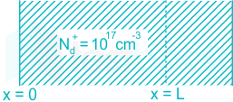
Consider a region of silicon devoid of electrons and holes, with an ionized donor density of Nd+=1017;cm3.{\rm{N}}_{\rm{d}}^ + = {10^{17}}{\rm{;c}}{{\rm{m}}^{ - 3}}. The electric field at x = 0 is 0V/cm  and the electric field at x = L is 50 kV/cm in the positive x-direction. Assume that the electric field is zero in the y and z directions at all points.

Given q=1.6×10¹⁹\rm q = 1.6 × 10^{−19} coulomb, ϵo=8.85×10¹⁴F/cm,ϵr=11.7\rm \epsilon_o = 8.85 × 10^{−14} F/cm, \epsilon_r = 11.7 for silicon, the value of L(in nm)\rm L( in \ nm) is ________.

48

Consider a long-channel NMOS transistor with source and body connected together. Assume that the electron mobility is independent of 𝑉𝐺𝑆 and 𝑉𝐷𝑆. Given, gm = 0.5 𝜇A/V for 𝑉𝐷𝑆 = 50 mV and 𝑉𝐺𝑆 = 2 V,

gd = 8 𝜇A/V for 𝑉𝐺𝑆 = 2 V and 𝑉𝐷𝑆 = 0 V,

Where \({{\rm{g}}{\rm{m}}} = \frac{{\partial {{\rm{I}}{\rm{D}}}}}{{\partial {{\rm{V}}{{\rm{GS}}}}}}\)  and \({{\rm{g}}{\rm{d}}} = \frac{{\partial {{\rm{I}}{\rm{D}}}}}{{\partial {{\rm{V}}{{\rm{DS}}}}}}\) 

The threshold voltage (in volts) of the transistor is ________.

49

The figure shows a half-wave rectifier with a 475 𝜇F filter capacitor. The load draws a constant current 𝐼𝑂 = 1 A from the rectifier. The figure also shows the input voltage 𝑉𝑖, the output voltage 𝑉𝐶 and the peak-to-peak voltage ripple 𝑢 on 𝑉𝐶. The input voltage 𝑉𝑖 is a triangle-wave with an amplitude of 10 V and a period of 1 ms.

The value of the ripple 𝑢 (in volts) is ________

50

In the opamp circuit shown, the Zener diodes Z1\rm Z_1 and Z2\rm Z_2 clamp the output voltage Vo\rm V_o to +5 V\rm +5 \ V or 5 V\rm −5 \ V. The switch S is initially closed and is opened at time t = 0.

The time t=t1\rm t = t_1 (in seconds) at which Vo\rm V_o changes state is ________.

51

An opamp has a finite open-loop voltage gain of 100. Its input offset voltage Vios (= +5mV) is modeled as shown in the circuit below. The amplifier is ideal in all other respects. Vinput is 25 mV.

The output voltage (in millivolts) is _________.

52

An 8 Kbyte ROM with an active low Chip Select input(CS)\left( {\overline {{\rm{CS}}} } \right) is to be used in an 8085 microprocessor-based system. The ROM should occupy the address range 1000H to 2FFFH. The address lines are designated as 𝐴15 to 𝐴0, where 𝐴15 is the most significant address bit. Which one of the following logic expressions will generate the correct CS\overline {{\rm{CS}}} signal for this ROM?

  1. ((a))

    A15 + A14 + (A 13 . A12 + A̅13 . A̅ 12)

  2. ((b))

    A15 . A14 . (A13 + A12)

  3. ((c))

    A̅15 . A̅ 14 . (A 13 . A̅12 + A̅13 . A12)

  4. ((d))

    A̅15 + A̅14 + (A13 . A12)

Show Answer
Answer: ((a))

A15 + A14 + (A 13 . A12 + A̅13 . A̅ 12)

Given address range: 1000 H to 2FFF

∴ Total No. of address lines = 13 i.e.  \(\begin{array}{*{20}{c}} {2{\rm{FFF}}}\ {\underline {1000} }\ {1{\rm{FFF}}} \end{array}\)

(1FFF)H = (0001 1111 1111 1111)2 = 13 address lines

i.e. \(\begin{array}{*{20}{c}} {{{\rm{A}}{15}}}&{{{\rm{A}}{14}}}&{{{\rm{A}}{13}}}&{{{\rm{A}}{12}}}&{{{\rm{A}}{11}}}&{{{\rm{A}}{10}}}& \cdots &{{{\rm{A}}_2}}&{{{\rm{A}}1}}&{{{\rm{A}}0}}&{}\ 0&0&0&1&0&0&{}&0&0&0&{ = {{\left( {1000} \right)}{\rm{H}}}}\ {}&{}& \vdots &{}&{}& \vdots &{}&{}&{}&{}&{}\ 0&0&1&0&1&1&{}&1&1&1&{ = {{\left( {2{\rm{FFF}}} \right)}{\rm{H}}}} \end{array}\)

i.e. \(\begin{array}{*{20}{c}} {{{\rm{A}}{15}}}&{{{\rm{A}}{14}}}&{{{\rm{A}}{13}}}&{{{\rm{A}}{12}}}\ 0&0&0&1\ 0&0&1&0 \end{array}\)

To provide CS\overline {{\rm{CS}}} as low, the condition is

A15 = A14 = 0 and A13 = A12 = (01) or (10)

i.e. A15 = A14 = 0 and A13 , A12 shouldn't be (11) , (00)

Thus it is A15 + A14 + (A 13 . A12 + A̅13 . A̅ 12)

Hence option (1) is correct

53

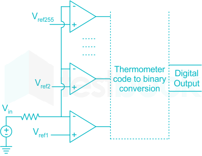
In an N bit flash ADC, the analog voltage is fed simultaneously to 2𝑁 − 1 comparators. The output of the comparators is then encoded to a binary format using digital circuits. Assume that the analog voltage source Vin (whose output is being converted to digital format) has a source resistance of 75 Ω as shown in the circuit diagram below and the input capacitance of each comparator is 8 pF.

The input must settle to an accuracy of 1/2 LSB even for a full-scale input change for proper conversion. Assume that the time taken by the thermometer to the binary encoder is negligible.

If the flash ADC has 8-bit resolution, which one of the following alternatives is closest to the maximum sampling rate?

  1. ((a))

    1 megasamples per second

  2. ((b))

    6 megasamples per second

  3. ((c))

    64 megasamples per second

  4. ((d))

    256 megasamples per second

Show Answer
Answer: ((a))

1 megasamples per second

For an N bit flash type converter, the number of comparators required is 2N1{2^{\rm{N}}} - 1

So, number of capacitors required for an 8 bit flash convertor is 281=255.{2^8} - 1 = 255.

Since all capacitors are in parallel, total capacitance C=255×8;pF=2.04;nF.{\rm{C}} = 255 \times 8{\rm{;pF}} = 2.04{\rm{;nF}}.

So the input time constant τ=RC=75Ω×2.04;nF=153;nsec{\rm{\tau }} = {\rm{RC}} = 75{\rm{\Omega }} \times 2.04{\rm{;nF}} = 153{\rm{;nsec}}

The input must settle within 12\frac{1}{2} LSB. Now, \(\frac{1}{2}{\rm{LSB}} = \frac{1}{2} \times \frac{1}{{{2^{\rm{N}}} - 1}}{{\rm{V}}{{\rm{in}}}} = {\left. {\frac{{{{\rm{V}}{{\rm{in}}}}}}{{510}}} \right|_{{\rm{N}} = 8}}\)

So, voltage required by the capacitor to settle within 12LSB\frac{1}{2}{\rm{LSB}} is \({{\rm{V}}{\rm{c}}} = {{\rm{V}}{{\rm{in}}}} - \frac{{{{\rm{V}}_{{\rm{in}}}}}}{{510}}\)

Now voltage across capacitor is given by \({{\rm{V}}{\rm{c}}}\left( {\rm{t}} \right) = {{\rm{V}}\infty } + \left( {{{\rm{V}}{\rm{o}}} - {{\rm{V}}\infty }} \right){{\rm{e}}^{ - \frac{{\rm{t}}}{{\rm{\tau }}}}}\).

We have \({{\rm{V}}\infty } = {{\rm{V}}{{\rm{in}}}}\), \({{\rm{V}}{\rm{o}}} = 0\). Substituting we have, \({{\rm{V}}{\rm{c}}}\left( {\rm{t}} \right) = {{\rm{V}}{{\rm{in}}}} + \left( {0 - {{\rm{V}}{{\rm{in}}}}} \right){{\rm{e}}^{ - \frac{{\rm{t}}}{{\rm{\tau }}}}}\)

\(\begin{array}{l} \Rightarrow {{\rm{V}}{{\rm{in}}}} - \frac{{{{\rm{V}}{{\rm{in}}}}}}{{510}} = {{\rm{V}}_{{\rm{in}}}}\left( {1 - {{\rm{e}}^{ - \frac{{\rm{t}}}{{\rm{\tau }}}}}} \right)\ \left( {1 - {{\rm{e}}^{ - \frac{{\rm{t}}}{{\rm{\tau }}}}}} \right) = \frac{{509}}{{510}}\ \Rightarrow {\rm{t}} = - {\rm{\tau }}\ln \left( {1 - \frac{{509}}{{510}}} \right)\ \Rightarrow {\rm{t}} = 953.87{\rm{;nsec}} \end{array}\)

This is the time required to convert on set of data applied at the input.

So, sampling rate fs=1t=1.04;Msamplessec{{\rm{f}}_{\rm{s}}} = \frac{1}{{\rm{t}}} = 1.04{\rm{;M}}\frac{{{\rm{samples}}}}{{{\rm{sec}}}}

54

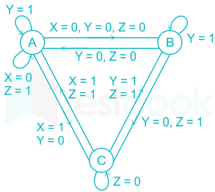
The state transition diagram for a finite state machine with states A, B and C, and binary inputs X,

Y and Z, is shown in the figure.

Which one of the following statements is correct?

  1. ((a))

    Transitions from State A are ambiguously defined.

  2. ((b))

    Transitions from State B are ambiguously defined.

  3. ((c))

    Transitions from State C are ambiguously defined.

  4. ((d))

    All of the state transitions are defined unambiguously.

Show Answer
Answer: ((c))

Transitions from State C are ambiguously defined.

From the state diagram we can write state table.

XYZPSNSPSNSPSNS
000ABBACC
001AABCCnot specified
010AABBCC
011AABBCB
100ACBACC
101ACBCCA
110AABBCC
111AABBCA/B (ambiguous)
<br>

So state C is ambiguously defined.

55

In the feedback system shown below  G(s)=1(s2+2s)\rm G(s)=\frac{1}{{\left( {{{\rm{s}}^2} + 2{\rm{s}}} \right)}}

The step response of the closed-loop system should have a minimum settling time and have no overshoot.

The required value of gain 𝑘 to achieve this is ________

56

In the feedback system shown below  G(s)=1(s+1)(s+2)(s+3)\rm G(s)=\frac{1}{{\left( {{\rm{s}} + 1} \right)\left( {{\rm{s}} + 2} \right)\left( {{\rm{s}} + 3} \right)}}:

The positive value of 𝑘 for which the gain margin of the loop is exactly 0 dB and the phase margin of the loop is exactly zero degrees is ________.

57

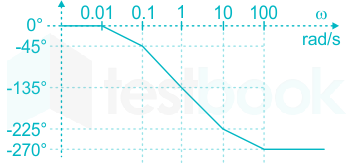
The asymptotic Bode phase plot of G(s)=K(s+0.1)(s+10)(s+p1)\rm G(s)=\frac{{\rm{K}}}{{\left( {{\rm{s}} + 0.1} \right)\left( {{\rm{s}} + 10} \right)\left( {{\rm{s}} + {{\rm{p}}_1}} \right)}},  with K and 𝑝1 both positive, is shown below.

The value of 𝑝1 is ________.

58

An information source generates a binary sequence {𝛼𝑛}. 𝛼𝑛 can take one of the two possible values −1 and +1 with equal probability and are statistically independent and identically distributed. This sequence is precoded to obtain another sequence {𝛽𝑛}, as 𝛽𝑛=𝛼𝑛+𝑘𝛼𝑛3\rm 𝛽_𝑛 = 𝛼_𝑛 + 𝑘 𝛼_{𝑛−3} . The sequence {𝛽𝑛} is used to modulate a pulse X(t)\rm X(t) to generate the baseband signal

\({\rm{X}}\left( {\rm{t}} \right) = \mathop \sum \limits_{\rm{n= - \infty}}^\infty {\rm{;\beta_ng}}\left( {{\rm{t}} - {\rm{nT}}} \right),\) where \({\rm{g}}\left( {\rm{t}} \right) = \left{ {\begin{array}{*{20}{c}} {1,}&{0 \le {\rm{t}} \le {\rm{T}}}\ {0,}&{{\rm{othervise}}.} \end{array}} \right.\)

If there is a null at 𝑓 = 13T\frac{1}{{3{\rm{T}}}} in the power spectral density of X(t)\rm X(t), then 𝑘 is ________

59

An ideal band-pass channel 500 Hz - 2000 Hz is deployed for communication. A modem is designed to transmit bits at the rate of 4800 bits/s using 16-QAM. The roll-off factor of a pulse with a raised cosine spectrum that utilizes the entire frequency band is ________

60

Consider a random process X(t)=3V(t)8\rm X(t) = 3V(t) − 8, where (𝑡) is a zero mean stationary random process with autocorrelation RV(τ)=4e5τ\rm R_{V}(\tau)=4e^{-5\left|\tau\right|}. The power in X(t)\rm X(t) is ________

61

A binary communication system makes use of the symbols “zero” and “one”. There are channel errors. Consider the following events:

𝑥0 : a "zero" is transmitted

𝑥1 : a "one" is transmitted

𝑦0 : a "zero" is received

𝑦1 : a "one" is received

The following probabilities are given:

P(x0)=12,;P(y0x0)=34 and;p(y0x1)=12.\rm P(x_0) =\frac{1}{2},{\rm{;P}}\left( {{{\rm{y}}_0}{\rm{|}}{{\rm{x}}_0}} \right) = \frac{3}{4}\ and;p\left( {{y_0}{\rm{|}}{x_1}} \right) = \frac{1}{2}..

The information in bits that you obtain when you learn which symbol has been received (while you know that a “zero” has been transmitted) is ________

62

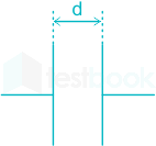
The parallel-plate capacitor shown in the figure has movable plates. The capacitor is charged so that the energy stored in it is 𝐸 when the plate separation is 𝑑. The capacitor is then isolated electrically and the plates are moved such that the plate separation becomes 2𝑑.

At this new plate separation, what is the energy stored in the capacitor, neglecting fringing effects?

  1. ((a))

    2𝐸

  2. ((b))

    √2𝐸

  3. ((c))

    𝐸

  4. ((d))

    𝐸/2

Show Answer
Answer: ((a))

2𝐸

Concept:  

Capacitance with the separation is r is given by C=ϵAr{{\rm{C}}} = \frac{{{\rm{\epsilon A}}}}{{{\rm{r}}}}

Application:

Capacitance when the separation is 2d.

C1=ϵA2d{{\rm{C}}_1} = \frac{{{\rm{\epsilon A}}}}{{2{\rm{d}}}}

Let the charge on plates be Q coulomb. Then, the energy of the capacitor with separation 2d is

E1=Q22C1 E1=Q22C1=Q22d2ϵA=Q2dϵA\begin{array}{l} {{\rm{E}}_1} = \frac{{{{\rm{Q}}^2}}}{{2{{\rm{C}}_1}}}\ {{\rm{E}}_1} = \frac{{{{\rm{Q}}^2}}}{{2{{\rm{C}}_1}}} = \frac{{{{\rm{Q}}^2}2{\rm{d}}}}{{2{\rm{\epsilon A}}}} = \frac{{{{\rm{Q}}^2}{\rm{d}}}}{{{\rm{\epsilon A}}}} \end{array}

The energy of the capacitor with separation d is

Now,   C=AdE=Q2d2ϵA{\rm{C}} = \frac{{{\rm{A}}}}{{\rm{d}}} \Rightarrow {\rm{E}} = \frac{{{{\rm{Q}}^2}{\rm{d}}}}{{2{\rm{\epsilon A}}}}

E=Q2d2ϵA\Rightarrow {\rm{E}} = \frac{{{{\rm{Q}}^2}{\rm{d}}}}{{2{\rm{\epsilon A}}}}

Thus, we see E=12E1{\rm{E}} = \frac{1}{2}{{\rm{E}}_1}

E1=2E\Rightarrow {{\rm{E}}_1} = 2{\rm{E}}

63

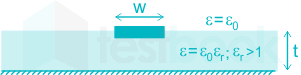
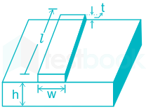
A lossless microstrip transmission line consists of a trace of width 𝑤. It is drawn over a practically infinite ground plane and is separated by a dielectric slab of thickness 𝑡 and relative permittivity 𝜀𝑟 > 1. The inductance per unit length and the characteristic impedance of this line are 𝐿 and 𝑍0, respectively.

Which one of the following inequalities is always satisfied?

  1. ((a))

    Z0>Ltε0εrw{Z_0} > \sqrt {\frac{{Lt}}{{{\varepsilon _0}{\varepsilon _r}w}}}

  2. ((b))

    Z0<Ltε0εrw{Z_0} < \sqrt {\frac{{Lt}}{{{\varepsilon _0}{\varepsilon _r}w}}}

  3. ((c))

    Z0>Lwε0εrt{Z_0} > \sqrt {\frac{{Lw}}{{{\varepsilon _0}{\varepsilon _r}t}}}

  4. ((d))

    Z0<Lwε0εrt{Z_0} < \sqrt {\frac{{Lw}}{{{\varepsilon _0}{\varepsilon _r}t}}}

Show Answer
Answer: ((b))

Z0<Ltε0εrw{Z_0} < \sqrt {\frac{{Lt}}{{{\varepsilon _0}{\varepsilon _r}w}}}

Concept:

A lossless microstrip transmission line consists of a trace of width ‘w’ as shown:

The characteristic impedance of the transmission line is given as:

Z0=LC{Z_0} = \sqrt {\frac{L}{C}}  , where C=εAdC = \frac{{\varepsilon A}}{d}

Application: As we know Z0=LC{Z_0} = \sqrt {\frac{L}{C}}  where C=εAdC = \frac{{\varepsilon A}}{d}

here d = t, A ≅ w, and ε = εeff

C=εeffwt\therefore C = \frac{{{\varepsilon _{eff}}w}}{t}

The above is the actual capacitance, with no fringing taken into account.

Z0=Lεeffwt=L.tw;εeff\therefore {Z_0} = \sqrt {\frac{L}{{\frac{{{\varepsilon _{eff}} \cdot w}}{t}}}} = \sqrt {\frac{{L.t}}{{w;{\varepsilon _{eff}}}}}

Let the characteristic impedance of a practical transmission line be Z0’.

Since in practice, the capacitance C will be smaller than the actual capacitance due to the fringing effects, i.e.since εeff < ε0 εr, we can write:

Z0’ > Z0, i.e.

Z0<Ltε0εrw{Z_0} < \sqrt {\frac{{Lt}}{{{\varepsilon _0}{\varepsilon _r}w}}}

This is because the capacitance is inversely related to the characteristic impedance, i.e. smaller the C, larger is the impedance.

64

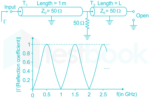
A microwave circuit consisting of lossless transmission lines T1 and T2 is shown in the figure. The plot shows the magnitude of the input reflection coefficient Γ as a function of frequency 𝑓. The phase velocity of the signal in the transmission lines is 2 × 10⁸ m/s.

The length 𝐿 (in meters) of T2 is ________

65

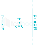
A positive charge q\rm q is placed at x=0\rm x = 0 between two infinite metal plates placed at x=d\rm x = −d and at x=+d\rm x = +d respectively. The metal plates lie in the yz plane.

The charge is at rest at t=0\rm t=0, when a voltage +V\rm +V is applied to the plate at d\rm – d and voltage V\rm −V is applied to the plate at x=+d\rm x = +d. Assume that the quantity of the charge q\rm q is small enough that it does not perturb the field set up by the metal plates. The time that the charge q\rm q takes to reach the right plate is proportional to

  1. ((a))

    d/V\rm d/V

  2. ((b))

    d/V\rm \sqrt d/V

  3. ((c))

    d/V\rm d/\sqrt V

  4. ((d))

    d/V\sqrt {{\rm{d}}/{\rm{V}}}

Show Answer
Answer: ((c))

d/V\rm d/\sqrt V

Concept:

from Newton’s equations of motion s=ut+12at2{\rm{s}} = {\rm{\vec ut}} + \frac{1}{2}{\rm{\vec a}}{{\rm{t}}^2}

Application:

We have potential difference in between plates is given by V(V)=2V{\rm{V}} - \left( { - {\rm{V}}} \right) = 2{\rm{V}}

Electric field in between plates, E=2V2d=Vd{\rm{E}} = \frac{{2{\rm{V}}}}{{2{\rm{d}}}} = \frac{{\rm{V}}}{{\rm{d}}}

Force on change Q, F=QE=QVd{\rm{F}} = {\rm{QE}} = \frac{{{\rm{QV}}}}{{\rm{d}}}

Let the charge Q\rm Q be of mass m\rm m. then acceleration experienced by it,

a=FM=QVmd{\rm{a}} = \frac{{\rm{F}}}{{\rm{M}}} = \frac{{{\rm{QV}}}}{{{\rm{md}}}}

Now, the charge has to cover distance d\rm d before it reaches the right plate with initial velocity zero. So, from Newton’s equations of motion we have, 

s=ut+12at2{\rm{s}} = {\rm{\vec ut}} + \frac{1}{2}{\rm{\vec a}}{{\rm{t}}^2}

 u=0,;s=d{\rm{u}} = 0,{\rm{;s}} = {\rm{d}} and a=qVmd{\rm{a}} = \frac{{{\rm{qV}}}}{{{\rm{md}}}}

d=12(qVmd)t2 t2=2qmdqV t2=2d.md9V t=2mqdV\begin{array}{l} \Rightarrow {\rm{d}} = \frac{1}{2}\left( {\frac{{{\rm{qV}}}}{{{\rm{md}}}}} \right){{\rm{t}}^2}\ \Rightarrow {{\rm{t}}^2} = \frac{{2{\rm{qmd}}}}{{{\rm{qV}}}}\ {{\rm{t}}^2} = \frac{{2{\rm{d}}.{\rm{md}}}}{{9{\rm{V}}}}\ \Rightarrow {\rm{t}} = \sqrt {\frac{{2{\rm{m}}}}{{\rm{q}}}} \cdot \frac{{\rm{d}}}{{\sqrt {\rm{V}} }} \end{array}

Thus, tdV{\rm{t}} \propto \frac{{\rm{d}}}{{\sqrt {\rm{V}} }}

Attempt this paper under real exam conditions

Timed interface, section switching, instant scoring, and question-by-question analytics — free.

Start Timed Attempt